Will there be a PCB design to share as there seems to be some aspects that could be tricky for optimal performance?
Not that tricky -- if it can be made to work on solderless breadboard all you need is some care in layout.
Attachments
In the above Resr can be jumpered, I think that if the output cap has ESR> 60 milliOhm the thing is stable. L1 is the ferrite bead -- can be put on the emitter leg of Q1.
I defer to LV who figured this thing out.
For some reason I am having pain trying to create a low Z outpath, the software isn't allowing me to attach a polygon to a specific net...
I defer to LV who figured this thing out.
For some reason I am having pain trying to create a low Z outpath, the software isn't allowing me to attach a polygon to a specific net...
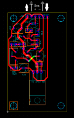
Jack, the two yellow routes to Q2-base seem to have a weency little air gap between them in #122. Could that give your software heartburn?
Also: rotating L1 90 degrees clockwise so it is near D2 anode, might be 0.001% closer to the ideal Kelvin connection in the schematic.
Also: rotating L1 90 degrees clockwise so it is near D2 anode, might be 0.001% closer to the ideal Kelvin connection in the schematic.
Last edited:
Mark, thanks for pointing that out!
I am getting software heartburn from my inability of creating a lower impedance route for the output node. For some reason I can't attach the copper polygon to the desired net. (It's a fully authorized version). (NOW FIXED") )
)
I have some SMT LM317 and LM337, and will probably use these.
I am getting software heartburn from my inability of creating a lower impedance route for the output node. For some reason I can't attach the copper polygon to the desired net. (It's a fully authorized version). (NOW FIXED
)I have some SMT LM317 and LM337, and will probably use these.
Last edited:
With the layout I adopted on the perfboard, the regulator tolerates a 20mΩ output cap without instability.In the above Resr can be jumpered, I think that if the output cap has ESR> 60 milliOhm the thing is stable. L1 is the ferrite bead -- can be put on the emitter leg of Q1.
I defer to LV who figured this thing out.
With the Kelvin connections, there is no need for particularly low impedance routes up to the point where they converge which is preferably at the point of load, thus normally outside the board.
That is the only way to achieve a <15µΩ output impedance.
If someone can suggest a very light and simplistic PCB drafting soft (not a dreadnought like Kicad), I can draw a PCB example based on my prototype (and I will correct the minor imperfections I have noticed).
If someone can suggest a very light and simplistic PCB drafting soft (not a dreadnought like Kicad), I can draw a PCB example based on my prototype (and I will correct the minor imperfections I have noticed).
Just take a snapshot and I can convert it to Ultiboard.
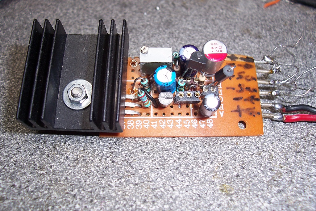
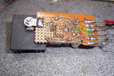
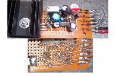
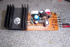
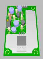
Here are the pics: I built my prototype in the shape of a compact, vertical plug-in module, because I thought it would be useful in the future, but other options are as valid.
Component side:
Copper side:
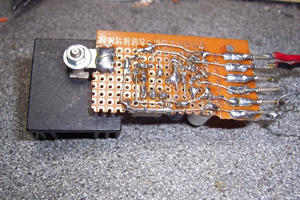
Both together with the copper side mirrored:

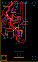
It is important to have a power path which is deterministic, well compensated and kept at a sufficient distance from the low-level circuitry: it is necessary to minimize parasitic induction effects.
This path is highlighted in green here:

The compensation of the currents is not perfect though: the distance between the hot and return paths is finite, and the GND side is the innermost, meaning it will couple more strongly to the correction amplifier.
That is where I made a mistake: I should have crossed the sense terminals, by moving the 10 ohm a little further for example:

It would also have been possible to make the crossing somewhere in the power path.
This means that a ground plane should be avoided, or used exclusively as an electrostatic shield, with just one connection point.
In fact, the PCB could be single-sided: this would allow DIYers to make it at home, and would force good layout practices.
My prototype is single-sided, except for two straps: the black wire on the component-side, and the small bridge on the solder side, but they are mainly a result of the pad matrix: they could be avoided in a real PCB.
Some additional remarks:
The socket in front of the transistor allows for a small capacitor between the collector and the GND sense.
It can be useful if the regulator is subjected to a HF ripple as large as the DC output.
It could be included -or not-
The hum-reduction R7 could also be implemented (my measurements were made without that resistor).
The output configuration is extremely important: the output cap C3 has to be placed as far as possible downstream, and both the load and the sense terminals must be directly connected to it.
Component side:
Copper side:
Both together with the copper side mirrored:
It is important to have a power path which is deterministic, well compensated and kept at a sufficient distance from the low-level circuitry: it is necessary to minimize parasitic induction effects.
This path is highlighted in green here:
The compensation of the currents is not perfect though: the distance between the hot and return paths is finite, and the GND side is the innermost, meaning it will couple more strongly to the correction amplifier.
That is where I made a mistake: I should have crossed the sense terminals, by moving the 10 ohm a little further for example:
It would also have been possible to make the crossing somewhere in the power path.
This means that a ground plane should be avoided, or used exclusively as an electrostatic shield, with just one connection point.
In fact, the PCB could be single-sided: this would allow DIYers to make it at home, and would force good layout practices.
My prototype is single-sided, except for two straps: the black wire on the component-side, and the small bridge on the solder side, but they are mainly a result of the pad matrix: they could be avoided in a real PCB.
Some additional remarks:
The socket in front of the transistor allows for a small capacitor between the collector and the GND sense.
It can be useful if the regulator is subjected to a HF ripple as large as the DC output.
It could be included -or not-
The hum-reduction R7 could also be implemented (my measurements were made without that resistor).
The output configuration is extremely important: the output cap C3 has to be placed as far as possible downstream, and both the load and the sense terminals must be directly connected to it.
Attachments


This is going to be difficult.... conveying simple graphic concepts with just words is not easy
It would be far simpler if I designed the thing myself, so I renew my question: can someone suggest a very basic and rudimentary drafting program?
It might be crude, but certainly no cruder than Paint used for that purpose.
Anyway, here is a correction attempt.
Note that the vertical form factor is not compulsory at all: a regular PCB with a left-> right power flow could work equally well, provided the basic requirements are met: a well defined power flow, sufficiently distant from the rest, with the hot and return conductors as close as practical for the whole path.
The essential point is: no loop area within this path
The corrected version attempts to do this, but not properly: the track are not as close as they should, and they should be thicker too
Attachments
It would be far simpler if I designed the thing myself, so I renew my question: can someone suggest a very basic and rudimentary drafting program?
expresspcb is freeware -- the traces don't "tack" to the nets, so a little care is necessary, design rules are limited, but for this exercise it should be more than adequate.
i use it for small batches of boards.
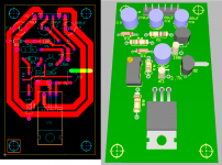
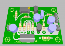
That is much better.
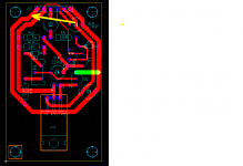
C5 could be moved closer to the 317, C3 slightly shifted towards the input posts and the sense terminals might need to be swapped, by routing Q1's emitter track under R6.
There is no explicit ferrite bead, but it can always be threaded directly on the emitter
C5 could be moved closer to the 317, C3 slightly shifted towards the input posts and the sense terminals might need to be swapped, by routing Q1's emitter track under R6.
There is no explicit ferrite bead, but it can always be threaded directly on the emitter
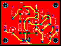
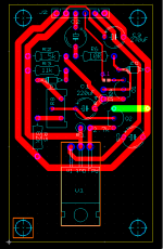
One last pass. By moving the "ground" to the outside it's much easier C3 is now near V_in, the ferrite bead (L1) can be placed on the bottom of the board, or on the emitter leg and the two via's jumpered.
the form factor for the some of the electrolytics is changed from ELKO5R2_5 to ELKO5R5 which leaves a little space to knit.
the form factor for the some of the electrolytics is changed from ELKO5R2_5 to ELKO5R5 which leaves a little space to knit.
Attachments
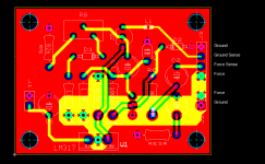
Thanks for your efforts, but there has been a small misunderstanding about C3 (my fault): I actually meant moving it close to J2 as a whole, not really the input section of J2.
If required, C2 can be pushed a little to the right to make room for it.
With these mods, I think this form factor is final and could be cast in bronze
Sorry for this unnecessary iteration
If required, C2 can be pushed a little to the right to make room for it.
With these mods, I think this form factor is final and could be cast in bronze
Sorry for this unnecessary iteration
Attachments
- Home
- Amplifiers
- Power Supplies
- D-Noizator: a magic active noise canceller to retrofit & upgrade any 317-based V.Reg.