Phase delay is : -Φ(ω)/ω
Group delay is : d(Φ(ω))/dω
Small correction
(Not directed anywhere in specific) I've long lost track of the threads direction and the arbitrary arguments about nomenclature versus "not caring what it's called but pay attention to the mechanisms". If "CFA" vs "VFA" is useful in term of giving a general idea of the system's behavior (from a family of topologies), then its served its purpose well enough. Aren't there more productive things to attack?
Like yourself, I have no idea what the debate points in this thread are about. It appears to me as more like an ego fight in which everybody is defending it's own trench and throwing grenades over the separation wall.
There seem to be a large amount of misunderstandings and confusion spread among various posters (about what "CFA" and "VFA" are, about small vs. large signal behavior, about models vs. a particular implementation, etc...).
I don't see anybody denying the existence of "CFAs" and their special small and large signal properties. The naming of "CFA" can, more or less academically, be rightfully debated, but ultimately who cares if it was already accepted by the industry? CFAs are here to stay, disregarding a rather confusing name chosen.
Personally, the only surprise was the original prof. Franco stance in defending CFAs (like they wold need any defense!).
Using two-port techniques to manipulate a CFA circuit into a series-shunt configuration is a popular alternative for the paper-and-pencil calculation of the loop gain T, but it fails on other vital issues, such as the correct representation of the type of feedback actually taking place.
What??? I thought the two-port analysis technique determines the feedback type, since the abstract two-port analysis doesn't make any assumptions about a specific implementation. But then, I'm currently way off the academic track, so perhaps he knows something about "feedback types" that I'm missing in the last 40 yeas or so. Anyway, I think I was able to mathematically re-construct the CFA known (and special) small signal properties by using the same input series, shunt output, two-port formalism that can be used in analyzing your favorite long tail pair VFA, and without any extra assumptions. This must tell something about the nature of CFAs.
Oh, and nothing is more "paper-and-pencil" prone than an abstract two-port analysis. Spice doesn't apply!
Last edited:
Well from your posts I get that your explanation or position depends on a delay existing between input signal and feedback signal.
No it doesn't. It was in reflection that an RC time constant exists at the Tz node that doesn't exist for input stimulus voltage feeding into the Thevenin equivalent resistance, this as connected to the opposing end to the V Thevenin output. The output, and therefore V Thevenin output, changes in response to the charging of C at the Tz node.
If we nevertheless agree that no time/phase delay exists is it thereupon also irrelevant for audio frequencies? Is it your position that there is no point in examining audio frequencies either, or anything beyond DC? Are you stating that the Middlebrook analysis is irrelevant in concluding the nature of a CFA or VFA, at frequencies beyond DC? Why are all the graphs included?
So it is absolutely imperative that this delay exists, otherwise your house of cards falls down. ==
I like the expression "house of cards" as oftentimes a single irreconcilable seed can do that... even taking down ones entire "being" in advance of perhaps ones reconstruction from the quantum of consciousness to correct.
Not at all... my argument begins from DC conditions. The irreconcilable seed that I perceive to exist is that the direction of output current from the current mirrors must match the direction of output current from the In- terminal and into R Thevenin.
Here is the infamous Martin Colloms article:-
A Future Without Feedback? | Stereophile.com
Here is another one that follows the same trend:-
Audio Note
Both talk about 'delays', feedback going around and around etc.
All crap.
Small correction
Phase delay is : -Φ(ω)/ω
Group delay is : -d(Φ(ω))/dω
Thank you.
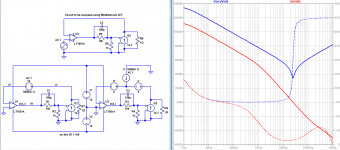
How would you interpret that claim in light of the fact that I can drive both CFA and VFA inputs with either current or voltage sources? Attached please find Middlebrook applied to a VFA to which a current source supplies feedback. Because of the use of the current source, Middlebrook demonstrates that c.f. predominates in this circuit, whose gain block is a VFA!
It turns out that if the impedance of the source seen by the feedback input exceeds that of the feedback input itself, c.f. predominates. Otherwise, v.f. does.
Looking at the schematics, I only understand that lower left part cannot work.
The voltage source in the feedback loop sees an infinite impedance from the current source, so that inverting input sees nothing.
I cannot see how to conclude anything of this scheme.
No it doesn't. It was in reflection that an RC time constant exists at the Tz node that doesn't exist for input stimulus voltage feeding into the Thevenin equivalent resistance, this as connected to the opposing end to the V Thevenin output. The output, and therefore V Thevenin output, changes in response to the charging of C at the Tz node.
I am sorry but no idea what your point is here. Surely the Tz RC-time exists for any signal at the Tz node? And of course, the Tz node being the output of a current source, the voltage changes exponentially according to the RC? Am I missing something here?
If we nevertheless agree that no time/phase delay exists is it thereupon also irrelevant for audio frequencies?
You are confusing things again. Of course there is phase shift in an amp, nobody in his right mind would deny that. And as has been stated repeatedly, the signal delay through the amp is in the order of a nanosec which means that the feedback is instantaneous at audio frequencies. And it is precisely the facts that phase shift exists and feedback is instantaneous which leads to instability at higher frequencies. (Depending on conditions of course; no need for you or other wise guys to explain that it depends on gain and phase margin. Stay focused).
So again, not sure what your point is here.
BTW I get that 'phase delay' expression. I think it is an oxymoron, and confusing as hell, but accept that it exists....
Jan
Last edited:
Confusing at all : CFA. I've difficulties to accept that it exists.confusing as hell, but accept that it exists....
Which assertions do you consider to be “all crap”? 😛All crap.
Eg, You know that if the feedback loop contains a time delay then recycling of out of date info is a thing. Are you declaring this to be insignificant in audio or are you denying the whole recycling notion?
denying the whole recycling notion?
Yes, it belongs with first cycle distortion.
Eg, You know that if the feedback loop contains a time delay then recycling of out of date info is a thing.
Echo chamber (media - Wikipedia) 😉
Looking at the schematics, I only understand that lower left part cannot work.
The voltage source in the feedback loop sees an infinite impedance from the current source, so that inverting input sees nothing.
I cannot see how to conclude anything of this scheme.
I tip my hat to you - you are correct! To remedy the situation, I added a 1 Gohm resistor across the current sources. Please see the updated attachments.
Middlebrook supplies the conclusion: there is more current feedback than voltage feedback in this circuit. And yet we've used a VFA as the gain block! How can this be?
It is because of what I have said before: To a good approximation for high loop gains, the ratio of current to voltage feedback at the inverting input of a circuit is a ratio of impedances: that of the feedback network (1Gohm in this case) to that of the inverting input (less than 1Gohm.)
Middlebrook does not reveal circuit topology; it only presents the voltage and current loop gains from which we can infer the feedbacks as described in the article I referred to.
Attachments
A demonstration of how the distributed nature of a real device can mimic a delay. This is a 5 stage R/C lowpass (1K and 2000pF) compared to 5K and 10000pF. This is grossly exaggerated a transistor like this would not even have 100kHz ft. If you saw this on a scope you would call it a delay but all ten devices have at least some current flowing instantaneously with applied step.
Attachments

I believe you are making a big mistake. Vf is an independent signal where it seems that you interpret it a Vf(eedback), but it is the stimulus itself.
Sorry not to get back earlier Hans... so much to think about. This was in reference to the EDN's article in I believe Figure 3, suggesting the Vf was the feedback voltage of a non-inverting amplifier as feeding Rf and Rg being shown in the feedback path. The problem was that Vf was 180 degrees out of phase with what would have appeared as Vf output. Being inverted, Vf could only translate to input current stimulus of an inverting amplifier. The article claimed this represented current feedback when in fact it was showing input stimulus current as a proof this represented current feedback.
Figure 4 is an example how to verifying open-loop transimpedance gain z(jf), feedback factor β(jf), and loop gain T(jf) in a CLOSED LOOP system.
In the PDF you have added, you are stimulating the In+ with a square wave. Totally different from fig 3 and 4 you are referring to.
As I suspected before, you are telling one thing but doing the opposite.
Sorry for the confusion... these PDF's weren't intended to be necessarily connected. My 35 year background in creating 100's of electronic devices and networks never involved explaining anything to anyone, hence I can sporadically switch gears in some understood connection as knowing to myself, yet be completely confusing to others trying to follow along.
In the brevity Figure 4 is only intended to identify what a feedback system will have to contend with... nothing more. I hope to provide more detail as time goes on. Thanks Hans
Good. Then this is my main point: Because the collector current is almost exactly equal to the emitter current which is equal to the current through Rg minus the current from the output stage, we have current feedback.
"almost exactly equal" : excellent !
This is absolutly not a proof of current feedback but a simple application of Kirchhoff law on In- node.
Current feedback cannot explain the ratio between "gm*Vbe" and "Vce/Ro" current in the input device. Voltage feedback does.
I wrote almost the same thing in that thread before knowing the existence of MDIT.Please note that Middlebrook's DIT will tell you that voltage and current feedback co-exist in CFA's, but that current feedback usually predominates.
You wrote "electron flow"This is why I use the term "signal current" to distinguish it from "bias current."
See attached.A transconductor requires at least three terminals to operate: two for control and at least one additional dedicated exclusively to the signal being controlled. A resistor and the Early Effect that it models are two-terminal entities. A resistor is no more a transconductance than it is a transresistance.
Let us distinguish between "current feedback" and "CFA". Middlebrook does not tell you whether you have a CFA, the name of which has been assigned by industry to a gain block with a specific topology. Middlebrook tells you whether current or voltage feedback predominates at a specific point in given circuit. Does this distinction make sense? I shall assume that you accept MDIT unless you say otherwise.
What are the criteria ? Who established it ? Who accepted it ?
See attached. Current on demand is not inherent in CFA.I'm not sure what you mean by "single device input." To me, by definition, a CFA's inverting input is connected to emitters/sources/cathodes. Current on demand is inherent in such a connection. And as long as the impedance of the inverting input is less than that of the impedance of the feedback network that that input sees, bandwidth can be held more or less constant as closed loop gain is varied. These characteristics are inherent in every CFA. They are not inherent in VFAs.
Constant bandwidth is easy to obtain with VFA, as current on demand.
Attachments


I hardly think your circuit is representative. Would you compensate a practical amplifier like that - VFA or CFA?
Its not surprising you have 'COD' like behaviour. You simply shunted some of the current mirror output to ground via C1 (4.7nF!?), so the front end is driving hard to try to recover the shunted current via Rf. If you do that to a classic VFA you get the same behaviour but the output of the VAS slews because the LTP tail current is fixed i.e. one half of the LTP is likely to turn off. What you have demonstrated here is that if you **** the compensation, you can get 'COD'.
There is no argument that there are tweaks to the VFA topology that will give it some gain bandwidth independence and high slew rates. This is why we should be clear about what we are discussing. There is certainly a big overlap in the two topologies wrt to behaviour as the (open) loop gain is raised. But, to try to sort this whole CFA vs VFA thing out by arguing about the behaviour in the overlap area to my mind seems a waste of time.
But, the question remains, is your circuit a VFA or a CFA?
Last edited:
But, the question remains, is your circuit a VFA or a CFA?
It could behave, small signal, like a CFA, but for lower closed loop gains (that is, lower R3/R2 ratio). Try R3=150 ohm and you'll get it.
For the R3/R2 as in the schematic it will likely behave (small signal) as a VFA.
The compensation is indeed poorly chosen; I would rather connect C1 between the Q2 collector and the Q1 emitter, resulting in a Faroudja compensation schema, but of course, more analysis is required. If C1 is connected as Faroudja compensation (and the amp is stable), then the (large signal) "current on demand" feature is guaranteed.
Or at least add a resistor in series with C1 to make a lead-lag compensation.
Of course it not representative of a realistic amplifier.
This caricatural scheme is to demonstrate that "current on demand" is not inherent to so called CFA but only to those which have a diamond (or similar) input.
Of course yes.
Gain bandwidth independance is obtained by playing with Rg resistor.
You have the same result by playing with the emitter resistor in a LTP or a double diamond.
Double diamond VFA allows same slew rate as so called CFA.
This caricatural scheme is to demonstrate that "current on demand" is not inherent to so called CFA but only to those which have a diamond (or similar) input.
There is no argument that there are tweaks to the VFA topology that will give it some gain bandwidth independence and high slew rates.
Of course yes.
Gain bandwidth independance is obtained by playing with Rg resistor.
You have the same result by playing with the emitter resistor in a LTP or a double diamond.
Double diamond VFA allows same slew rate as so called CFA.
Attachments
My question as to whether is was CFA or VFA was rhetorical 😉.
Agree with your comp proposal - I used it on the sx and nx amps. For high loop gain CFA I use other approaches.
Agree with your comp proposal - I used it on the sx and nx amps. For high loop gain CFA I use other approaches.
- Home
- Amplifiers
- Solid State
- Current Feedback Amplifiers, not only a semantic problem?