
There s nothing more to extract from this amp topology even with a regular high beta AB class complementary OS and TMC,
there s much greener pastures to graze, kudos to the predecessors but our aim should be to outmach the ultra high NFB
class D amps so analog wont go the way of the dodo.
And thanks as well, i always have a coffee in my desk.😉
there s much greener pastures to graze, kudos to the predecessors but our aim should be to outmach the ultra high NFB
class D amps so analog wont go the way of the dodo.
And thanks as well, i always have a coffee in my desk.😉
Attachments

The so called FFWD resistance should be treated the other way around, that is, as some NFB return path resistance.
Since the VAS has very high output Z this resistance totaly AC tie the OS output to the VAS output, and as such
the OS is enclosed in the miller NFB local loop, that s reminiscent of TMC but on a larger BW and OS output to VAS input
return ratio scales.
In the meantime,
I have found a fairly simple mathematical proof for wahab's bold thesis that the entire OPS is located within the local capacitive negative feedback, the so-called Miller loop.
That's why I'm now adding an apology to @wahab to the end, it was short-sighted of me to question your thesis. Please excuse my narrow-mindedness, you were right from the start. I admit that Quad & all those who want to prove CD with power using the example of the 405 or the 909 are mistaken. The good THD data of this Quad family is due to the completely free idle amplification /open-loop-gain of the system.
It's almost unbelievable, or rather we just want to believe in the miracle of feedforward error compensation. But in the case of the Quad family, it's not based on this at all - the secret is very well concealed.
Wasn't it even Douglas Self himself who dismissed the possibilities of frequency response compensation involving the OPS in the Miller loop as practically unrealizable because it was unstable?
Again:
I'm very sorry for that little dumb battle.
HBt.
- First amp is a normal feedback amp, no CD, just feedback.
- Second is the same with CD. Full cancellation of current dumper's distortion.
- Third is the same with a separate buffer for the FFWD resistor, so no feedback from the output of the current dumper here. The cancellation is the same as in the second amp with CD.
- Fourth is the same with the buffer and FFWD resistor turned the other way around, so no FFWD, just extra feedback. No cancellation, and additional feedback from the output of the current dumper make no difference.
What’s the output of an ideal amplifier that is with miller compensation? Will that be identical to the inputs? The answer is NO. The output is just an integral of all the error in the past. It is not following the positive input strictly.
The integral of all the error signal is not we want. We want the output signal to be exactly like the input signal. Here is the feed forward resistor into play. The same error gets integral on the feedforward resistor through the RL network also. If you subtract the voltage of the resistor from the voltage of the miller cap, you get the exact signal that is on the positive input pin. Of course, the bridge has to be balanced to make it work.
The integral of all the error signal is not we want. We want the output signal to be exactly like the input signal. Here is the feed forward resistor into play. The same error gets integral on the feedforward resistor through the RL network also. If you subtract the voltage of the resistor from the voltage of the miller cap, you get the exact signal that is on the positive input pin. Of course, the bridge has to be balanced to make it work.
The examples in my above post used pure voltage controlled current sources, so perhaps you might think that the capacitive feedback over the OPS is not there. For your enjoyment, I cobbled together examples with voltage controlled current sources with finite transconductance and local capacitive feedback. They work the same except I did not get full cancellation here for the 2nd and 3rd amps. The pattern, however, is identical - extra feedback from the load via the resistor in the amp no.4 makes no difference, while feedforwarding via the same resistor in no.2 and no.3 effectively eliminates the distortion of the OPS.


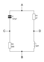
The reasoning, i.e. the proof for X, starting from X itself is great. What numerical values did the resistors and L and C have in the models and how do they relate to each other?
Basically, we are only interested in a frequency range from quasi DC to 7kHz.
{
47Ohm
3µH
127.7pF
500Ohm
}
kindly,
HBt.
Basically, we are only interested in a frequency range from quasi DC to 7kHz.
{
47Ohm
3µH
127.7pF
500Ohm
}
kindly,
HBt.
A real amplifier (the Amp alone) should prove that it strictly follows the (ideal CD) model. The model cannot prove that number 405 really works according to the CD principle.
The model alone proves that the model, the idea works.
🙄
The HOW, the (present) mechanism is of interest, nothing else.
The model alone proves that the model, the idea works.
🙄
The HOW, the (present) mechanism is of interest, nothing else.
Abstract models have their limitations, although I often find that a focus on implementation detail obscures a broader idea. In particular, when discussing Walker's feedforward idea, it is all but impossible not to mention the Quad 405 and its brethren, even though the OP wanted to make something different 😉
As for values, in the above examples, they are arbitrary and follow the L=RRC formula. In the first set of examples, the T used in the transconductance formula is simply T=RC. In the second set, L has an additional series impedance of 1/G. Note how using a VCCS instead of a voltage source eliminates the value of FFWD R from the equations.
As for values, in the above examples, they are arbitrary and follow the L=RRC formula. In the first set of examples, the T used in the transconductance formula is simply T=RC. In the second set, L has an additional series impedance of 1/G. Note how using a VCCS instead of a voltage source eliminates the value of FFWD R from the equations.
👍Note how using a VCCS instead of a voltage source eliminates the value of FFWD R from the equations.
That's exactly how it is!
______________________________
R(ff) * R(fb) = L / C
= jOmega * (XL - XC)
-------------------------------------
Last edited:
jxdkingthough the OP wanted to make something different 😉
would like to apply the Quad's principle of the CD; with an ideal OP as the first stage, this should be error correction and supplier at the same time. In this case, we can consider our op-amps as a practically ideal voltage source.
This is the ...

Residual Voltage, amplified by a factor of 10 so that we can see anything at all (for example in the time domain - on our analog oscilloscope, please do not use a DSO!).
Please imagine this in the time and frequency plane as a voltage above the FFWR. The power consumption is exactly 15.5Wrms in my example, the frequency of the sine function is 3kHz.
Apart from the obvious, the question immediately arises as to what the magic of the CD wizard is supposed to correct now?
The separate push-pull output stage operates in B mode according to Douglas Self's diction and is optimally preset at 60mAdc.
#
Should I turn the BIAS down to zero? Never!
Iq < 10mA

and 125mWrms

If you are looking for the actual time signal, this represents a horizontal line parallel to the time axis. You may also consider two points of equal potential as a short circuit.
A deviation from the line would be the temporal error; an error [ e(t) ] that does not exist cannot be corrected.
A feedforward resistor is of no use here.
and 125mWrms
If you are looking for the actual time signal, this represents a horizontal line parallel to the time axis. You may also consider two points of equal potential as a short circuit.
A deviation from the line would be the temporal error; an error [ e(t) ] that does not exist cannot be corrected.
A feedforward resistor is of no use here.
300Hz & 125mWrms

The difference is now clearly visible in the time domain, but in the spectrum (above) we cannot see any k3, k5, k7, k9 ..!
The difference is now clearly visible in the time domain, but in the spectrum (above) we cannot see any k3, k5, k7, k9 ..!
R(ff) * R(fb) = L / C
= jOmega * (XL - XC)
what a Freudian slip
Correction:
= jXL * -jXC
= jOmega*L times 1/jOmega*C
j(R(ff) / XC) = j(XL / R(fb))
jOmega * [R(ff) * C] = jOmega * [ L / R(fb)]
T=6ns
Then there is no more bridge and therefore no more current dumping -> OPS is now a full member of the Miller loop.Note how using a VCCS instead of a voltage source eliminates the value of FFWD R from the equations.
thx
alexcp
greetings,
HBt.
The "bridge" is still there. It's just that the value of a resistor connected in series with a current source makes no difference.
Care to explain how that Miller loop works?
Care to explain how that Miller loop works?
The situation at hand is not that simple, even if your statement is fundamentally completely correct.The "bridge" is still there. It's just that the value of a resistor connected in series with a current source makes no difference.
Only the modeling of the present topology of the Quad405 as a model amplifier to illustrate the so-called current dumper principle is wrong or completely inadequate.
In terms of control technology, what we are fabricating here is a nightmare.
Sure, but it's so obvious and completely open in front of you that the old adage: one only see what one want to see, hits the mark perfectly.Care to explain how that Miller loop works?
And as simple as the explanation and proof are, you need direct interaction with the questioner, a whiteboard and various colored pens ..! Anything else is not really sustainable.
HBt.
(I'm thinking about slaughtering the golden calf)
- Home
- Amplifiers
- Solid State
- Current Dumping with OPAMP