Has the question ever been asked - and answered - why the voltage amplification factor of the disguised single-ended quasi-complementary push-pull output stage is 11.5dB of all things?
For us today, the limitation means that, against our better judgment, we have to set up a defective power amplifier in order to apply the magical effect of the CD to it.
A different, testing approach would be better, namely not one of feasibility, but one of improvement.
#
Somehow I find it significant, but only as an aside, that the German and self-proclaimed expert M. Kühne could not cope with K. Snock's modification and had to design the power amplifier (with the magic amplification factor 1+50/18 ) completely symmetrically in order to achieve success.
regards,
HBt.
Psst
the load demands a very specific current and this must first be formed at the output-node by the current through the 47 Ohm branch and the current through the 3 µH branch. The first branch should provide the fully error-correcting current, while the second branch takes over the actual load current. This is the dumper, with a terrible wingspread diagram, i.e. distorted in the signal zero crossing, switching on and off, virtually unable to work. In a way, the idea (taken from another thread in this forum) that the dumper is switched on first is correct. But wrong in terms of system theory. It is better to start from the idea that everything works in parallel and simultaneously, but not always linearly.
To be honest, I now suspect that the well-known “old schooldesign”, the topology, was tinkered with until a circuit was created, the function of which was tried to be explained afterwards. Or, alternatively, they wanted to surgically couple the existing topology (by the skin of their teeth) with the theoretically known principle of error correction. Not in order to avoid any possible adjustment work, but to create a unique selling point.To do current dumping, there are 2 major requirements or limitations.
For us today, the limitation means that, against our better judgment, we have to set up a defective power amplifier in order to apply the magical effect of the CD to it.
A different, testing approach would be better, namely not one of feasibility, but one of improvement.
Clearly in order to have sufficient reserve for the effect of the hidden and obvious NFB. Of course, such a step is not resilient in any way. This is why the cascaded (single-ended) emitter follower follows on from the QUAD.1. It needs a very high gain and linear VAS. Quad uses a tripled Darlington configuration.
This consists of the complementary Darlington on the output side, or is tapped.2. The class A stages has to provide at least around 1% of the total output current.
That's exactly how it is.If that is over 50mA,(1% of 100W into 8 Ohm), it is not practical to use VAS to drive the feedforward resistor directly. That means over that, you need create another low distortion class A (at least AB) stage to drive the feedforward resistor.
#
Somehow I find it significant, but only as an aside, that the German and self-proclaimed expert M. Kühne could not cope with K. Snock's modification and had to design the power amplifier (with the magic amplification factor 1+50/18 ) completely symmetrically in order to achieve success.
regards,
HBt.
Psst
the load demands a very specific current and this must first be formed at the output-node by the current through the 47 Ohm branch and the current through the 3 µH branch. The first branch should provide the fully error-correcting current, while the second branch takes over the actual load current. This is the dumper, with a terrible wingspread diagram, i.e. distorted in the signal zero crossing, switching on and off, virtually unable to work. In a way, the idea (taken from another thread in this forum) that the dumper is switched on first is correct. But wrong in terms of system theory. It is better to start from the idea that everything works in parallel and simultaneously, but not always linearly.

Po=100W(peak)
Rl =8Ohm
28.3Vp
3.54Ap
The preamp (IPS) in disguise (the op-amp) must therefore boost the input signal to 7.5Vp so that 100W can come out at the rear - the Quad405 and its successor is a two-stage cramp /fighter.
Which partial reinforcement division would make the most sense? 1 to 1 or 10 to 1 ...! What is the permitted tolerance of the elements Z1, Z2, Z3 and Z4?
Addendum
for 100 watts RMS the IPS OP-Amp stage should be distortion-free, compression-free ... etc.pp. to around 11Vp.
Last edited:
The so called FFWD resistance should be treated the other way around, that is, as some NFB return path resistance.
Since the VAS has very high output Z this resistance totaly AC tie the OS output to the VAS output, and as such
the OS is enclosed in the miller NFB local loop, that s reminiscent of TMC but on a larger BW and OS output to VAS input
return ratio scales.
Prove is that if you add a TMC network then distorsion increase a lot, wich mean that the TMC net reduce the return ratio
from OS output to VAS input and increase it from VAS output to its input, hence, the distorsion cancellation is nothing else
than huge amount of NFB around the OS thanks to a totaly inclusive compensation loop.
Indeed the authors at Wireless world said that their analysis of error cancellation only apply at DC or at very low frequencies,
namely in the frequency range were the miller loop is of no effect and where the total NFB around the OS is at its peak,
wich mean that to get the same peak NFB at audio frequencies, and hence same error cancellation than at DC,
the OS has to be totaly enclosed in the miller loop.
@wahab
I've been thinking about your last post for a few hours now and trying to follow your train of thought, but I'm finding it a bit difficult at the moment. I'm wavering between agreeing and disagreeing.
Perhaps we should concentrate on the “Ludwig circuit” for analysis.
I've been thinking about your last post for a few hours now and trying to follow your train of thought, but I'm finding it a bit difficult at the moment. I'm wavering between agreeing and disagreeing.
Perhaps we should concentrate on the “Ludwig circuit” for analysis.
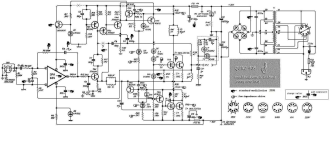
Attachments
I've got it 🙂
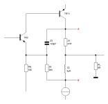
VAS only:
I have erased everything that could cloud or distract our view.

Let's just simulate the part (and time) when the push-pull output stage (the dumper), which is still forming, cannot be in play at all (or only in a rudimentary and very limited, distorting way).
It's a damn clever circuit after all.
HBt.
VAS only:
I have erased everything that could cloud or distract our view.
Let's just simulate the part (and time) when the push-pull output stage (the dumper), which is still forming, cannot be in play at all (or only in a rudimentary and very limited, distorting way).
It's a damn clever circuit after all.
HBt.
That's all about! Without the resulting frequency compensation scheme ..!
#
The only interesting point now is when and how does the dumper come into play ---> how does the dynamic output resistance of the entire circuit behave, how does the entire power amp react to naughty speaker impedances?
AC wise the 47R short the VAS output to the OS output, so the miller loop and its NFB enclose the OS as well.
This way there s 100dB NFB around the OS at all frequencies.
This way there s 100dB NFB around the OS at all frequencies.
Last edited:
AC wise the 47R short the VAS output to the OS output, so the miller loop and its NFB enclose the OS as well.
This way there s 100dB NFB around the OS at all frequencies.
It is obvious how the circuit works, I think that is no longer the point.
At the moment of zero crossing +/- a few millivolts, practically speaking, only the two-stage VAS (and the upstream OP amp, as well as the associated DC correction of the output) is working.
And
- in this combined characteristic range, we can also consider the same ac potentials, nodes A and B, to be virtually connected to each other.
- now the so-called feedforward resistor, namely Z1, is virtually in parallel with Z2 and in series with the load resistor demanding current, the loudspeaker.
I can still see neither a two-pole compensation nor a TMC.
As soon as the dumper, the connected push-pull output stage, comes into play, only then does the “take away error correction” get its chance to completely change the situation. But no one should now believe that this simplified description even comes close to a correct engineering picture.
HBt.
Attachments
Without you probably having realized it, the two nodes to the right and left of the 47Ohm resistor (maybe this is your term "short") are of course virtually equal (within frequency-dependent limits) - but also not, because the phase-shifted error voltage lies between two relevant nodes of our many equivalent circuit representation options ..!AC wise the 47R short the VAS output to the OS output, (...)
The Currentdumper number is no longer trivial as soon as we go into depth. But that's going way too far here in the forum, isn't it? Let's take a practical and simplified approach to the matter.
#
At the end of the day, the reward for our collective deliberations (brainstorming) should be a new, much better QUAD2025 - we can actually forget the OP amp variants for dummies, the title of this thread - that does and doesn't work.
Your point is based on the fact that TR9 is actually in C mode, so in the truest sense of the word it has to be switched on first, switching off happens automatically and incredibly quickly ..!
Mr. Walker's circuit is absolutely not stupid.
Let s describe the things otherwise.
The impedance at the QC output is 32 uR at 1kHz and 340 uR at 20kHz.
When OL the numbers are 250-260 mR at both frequencies.
Hence the total (G?)NFB around the OS is 78dB and 57dB respectively, 57dB GNFB at 20kHz is unheard of in usual miller
compensated amps.
The impedance at the QC output is 32 uR at 1kHz and 340 uR at 20kHz.
When OL the numbers are 250-260 mR at both frequencies.
Hence the total (G?)NFB around the OS is 78dB and 57dB respectively, 57dB GNFB at 20kHz is unheard of in usual miller
compensated amps.
Sorry, I can no longer follow you with your chosen abbreviations - what do you mean?The impedance at the QC output is 32 uR at 1kHz and 340 uR at 20kHz.
When OL the numbers are 250-260 mR at both frequencies.
QC ?
OL ? open loop - offene Schleife
f: 1kHz
255*10^-3 [V/A] / 32*10^-6 [V/A] = 7968.75
f: 20kHz = 2 * 10 * 1kHz
255*10^-3 / 340*10^-6 = 750
"QC" should now actually mean CL, i.e. closed loop- geschlossene Schleife ?! Tell me, how did you determine the output resistance in each case?
#
The rest of the riddle thrown in only shows that the OLG (in your example) falls at /with -20dB per decade - what a great miracle that is.
😱
QC quasi complementary
OL open loop
NFB negative feedback
GNFB global negative feedback
The same miracle as a very agressive and unreasonably set TMC or TPC.
OL open loop
NFB negative feedback
GNFB global negative feedback
The same miracle as a very agressive and unreasonably set TMC or TPC.
Last edited:
agree 🙂QC quasi complementary
OL open loop
NFB negative feedback
GNFB global negative feedback
You could perhaps see it that way, but I don't want to follow you on this point yet. Perhaps you could really go into detail about this, including all the example calculations (with calculation path). I think this could be very interesting for some readers.The same miracle as a very agressive and unreasonably set TMC or TPC.
For my part, I would like to stick with the circuit analysis of the Quad405 at the moment.
#
Yes, I admit that I can see too - and I'm sure we're getting close. All the way to full convergence.
kindly,
HBt.
However, this would then correspond to a huge damping factor - and this has yet to be explained by a complete circuit analysis. The upper switch TR9 alone cannot be the cause.The impedance at the QC output is 32 uR at 1kHz and 340 uR at 20kHz.
riq = 0.000032 Ohm up to 0.00034 Ohm
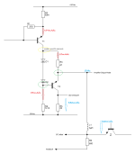
A first glance at the sketch below reveals the functions of the 47 Ohm feedforward resistor. Among other things, it ensures that an almost constant quiescent current flows through our lower play partner, which ensures a relatively constant bias voltage of 330mV (VBE of the NPN power transistor on the lower rail, not shown here). As a result of an ac current flowing through our load (sucking or squeezing in) ... - No, we don't have to go that far in our considerations, we can also simply modulate the base potential of the upper (final VAS PNP) BJT ac moderately. We move back and forth on the time function, the simplest is the sine. Let us consider the output node and bear in mind that it also follows the modulated base potential of the lower node (base electrode) in phase - it is an emitter follower and at the same time a dynamic current source for the upper VAS node. This results in a fairly large open-circuit amplification factor of this (now isolated) stage. At the same time, however, there is also an SRPP component, i.e. the output resistance is reduced compared to other variants - relatively (relatively) small. The 47 ohm resistor also has another task, namely that of a sensor function, as soon as the modulated potential, i.e. with our signal AC voltage, exceeds a defined point, the upper (an emitter follower) dumper slowly comes into play ..!
And only now does the number become interesting - all without any external load playing on the output node of the amplifier (namely pulling and pushing, pressing or sucking).
HBt.
And only now does the number become interesting - all without any external load playing on the output node of the amplifier (namely pulling and pushing, pressing or sucking).
HBt.
Attachments
DF is tied to the available NFB, if the OLG output Z is 1R and NFB at 1kHz is 100db then the CLG output Z
will be 10uR at 1kHz.
The path through the 47R will have 0.47mR output Z/1kHz, wich is much lower than the 20mR/1kHz through
the 3.3uH inductance.
So the inductance insulate the VAS + 47R output Z (= 0.47mR) from the OS lower output Z all while allowing the latter
to be enclosed in the miller loop since the inductance s 20mR is negligible compared to 47R when it comes to a NFB return path.
That could sound as a bizarre analysis but one way or another a distorsion cancellation cant exceed the correction
provided by a given amount of NFB, there s no way that say 60dB available NFB can reduce THD by say 80dB
comparatively to the OLG THD.
I ll do a sim with the same schematic + TMC later, so FFWD + TMC and also only TMC at same (half) class C Iq.
with OP-Amplifier as the name of the thread ...

#
Apart from that, we can now do a bit of math with your figures.
1) 78dB + 11.5dB = 89dB OLG
2) 57.5dB + 11.5dB = 69dB OLG
That's quite a lot for an amplifier from the 1970s, especially at f=20kHz. But again, not so unusual for a current feedback amplifier.
Now It is clear why a QUAD needs the unconditional input band limitation of less than 50kHz (as a rule of thumb). Jan Lohstroh and Matti Otala are turning over in their graves right now.
HBt.
It would be nice if you could clarify this point -wahab.Tell me, how did you determine the output resistance in each case?
#
Apart from that, we can now do a bit of math with your figures.
1) 78dB + 11.5dB = 89dB OLG
2) 57.5dB + 11.5dB = 69dB OLG
That's quite a lot for an amplifier from the 1970s, especially at f=20kHz. But again, not so unusual for a current feedback amplifier.
Now It is clear why a QUAD needs the unconditional input band limitation of less than 50kHz (as a rule of thumb). Jan Lohstroh and Matti Otala are turning over in their graves right now.
HBt.
- Home
- Amplifiers
- Solid State
- Current Dumping with OPAMP