I have already indicated the impedances of the nodes in terms of magnitude above. Now the puzzle of the magic error reduction can be easily solved, let's go!
Merry Christmas, I wish us all peaceful, calm and stress-free days,
HBt.
😍

A very last (unfortunately repetitive) note:
The static view, i.e. DC-like, is not identical to the dynamic view, i.e. AC-like. Please pay attention!
The static view, i.e. DC-like, is not identical to the dynamic view, i.e. AC-like. Please pay attention!
In the continuation on a previous aside... I also continued with the floating current mirroring theme and thought of starting a separate thread on this. I did some simulations with the help of Hans Polak, also showing me how to perform the distortion analysis in LTSpice.
To give the amplifier some stress I connected a 2 Ohm load and applied around 10VRMS (5A RMS) in the simulation, hence this produces about 50 watts into a 2 Ohm load. The screenshots show a multiple feedback loop arrangement using op-amps to illustrate some possibilities. Note that this restricts power for 8 Ohms loads being limited by the power supply limits of the op-amps. Of further note is that R4 and R8 (set at 0.025 Ohms) perform current limiting of the output MOSFET's by shunting the current sources connected to the gates. The values support the 7 Amp peaks in this simulation.
In a multiple feedback loop arrangement, this normally requires successively lowering the bandwidth as the loops expand outward, however because the current mirror feedback mechanism provides fast high current feedback in charging the high input and output capacitances of the MOSFET's this supports a triple loop network that can still manage about 90KHz at the 3 db intercept shown in the right screenshot. The screenshot on the left also shows the clean looking (though highly distorted) current waveforms of the output devices through the zero transition regions. Of note is the magnitude of current of each device passing through the zero transition, still maintaining the quiescent DC value (about 250mA) at 3 KHz to support the low distortion results shown in the upper right.
It should be noted that many parts were loosely selected from the LTSpice library, with transistors more critically selected for the complementary pairs in the mirrors. The output bipolar devices are 5A types and the inputs 0.5A types. This creates about a 5:1 current mirror ratio for the devices chosen as found by using simulations. Hence the input pair is running around 50mA (set by the current sources) and the output is tracking at about 250mA quiescent. Keep in mind that physical experimentation is necessary to realize more accurately the currents and also to determine the manner of thermal tracking in the turn on and of variance of the quiescent currents under load as well as the mechanical integration of the four bipolar making up the current mirrors.
The next step is usually to set up two mesh equations, both of which end with =0. We place the unloved error voltage (all non-linearities, etc. pp.) as a simplified source between the points AB; we also recognize this procedure in the old letters to the editor and short articles on the subject of current dumping. In the next step, we could equate the mesh equations and immediately recognize something algebraically, namely that the error voltage can always be eliminated 100%. In this case algebraically by subtracting the same term on both sides of the equation.
We immediately register a paradox, because formally there is no error at all. As we know, you cannot conjure up or even prove non-existence - this is identical to the today dilemma ..!
Apart from that, the scenario, the almost final step towards solving the problem, is similar to the quick proof results with the hint hidden as a footnote "that the 100% algebraic error elimination is only valid for f=0Hz, i.e. dc.
Whether transients are also to be excluded can now be implicitly imagined by everyone.
I am curious whether a useful approach to the miracle of error reduction can be solved with a vectorial (we call it a pointer) approach. Because in the steady state, everything seems to work perfectly, sin(omega t) moderately.
HBt.
Attachments
V_AB / V1

V_AB / V_C´C

V_AB / V_D_0V
with RL=1kOhm

V_AB / V_D_0V
with RL=100Ohm

V_AB / V_D_0V
with RL=10Ohm

V_B_0V / V_A_0V
with RL=10 Ohm

note:
all without Dumper TR9
V_AB / V_C´C
V_AB / V_D_0V
with RL=1kOhm
V_AB / V_D_0V
with RL=100Ohm
V_AB / V_D_0V
with RL=10Ohm
V_B_0V / V_A_0V
with RL=10 Ohm
note:
all without Dumper TR9
I can abbreviate the story and end with the quote from Mr. Walker himself, he said (from memory): R1 & L are practically parallel (i.e. virtual) to each other.The plots thickens.😉
This means in plain language that there is no CD principle at all.
Logical conclusion:
then the Composit VAOP stage is automatically in the so-called Miller loop. If C' is virtually identical to C (this is only possible if the ring is closed), then the situation changes even more to the disadvantage of the CD doctrine (the magic bridge).

then the Composit VAOP stage is automatically in the so-called Miller loop. If C' is virtually identical to C (this is only possible if the ring is closed), then the situation changes even more to the disadvantage of the CD doctrine (the magic bridge).
Unfortunately, unfortunately ... for definitive proof, not circumstantial evidence, we need the vectorial string currents IR1 & IL and their spectrum ... perhaps a pointer diagram which leads us to the sum current IRL.
Because "everything is in the loop" - and depending on the perspective taken, perhaps the CD principle proclaimed to this day really does exist?!
Who knows for sure? Our Christmas tale could end here.
Good night,
HBt.
Because "everything is in the loop" - and depending on the perspective taken, perhaps the CD principle proclaimed to this day really does exist?!
Who knows for sure? Our Christmas tale could end here.
Good night,
HBt.
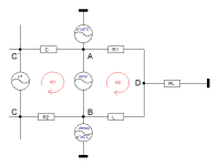
The paradox
We now know that nodes A and B are virtually regarded as a short circuit, but in reality they are not. Similarly, in our simplified network we transform the nodes C'&C into a single node and call it C. To the left of it we place an AC voltage source against ground, with the voltage V1. And now the network theory again gives us various options, freedom as to how we want to proceed. We can shift (keeping in mind that the isolated fault appears to arise between nodes A & B and remains there) - the superposition principle sends its regards.
1. bluntly we recognize two impedances, a complex resistor between C & (AB) and a second one between (AB) & D. From D to the reference potential (ground) lies our actual load Rload.
2. a bit of complex juggling leads to two therms that are identical in value, namely T1 & T2 (in the example 63.8ns - also called tau or time constants). Immediately we can determine the pointers and their angles, i.e. the |Z| * e^(+/-j phi), of course also the components, the real and the imaginary part.
Using the Laplace transform it is even easier, but that is irrelevant, because: we register a practically real resistance value of 500Ohm (with an angle of -2*10^-3°) for the left impedance and also 500Ohm (-0.000...6°) on the right - for f=1kHz, everything is real.
3. in the next step (procedure from left to right) we sketch an extremely simplified network with V1 - 500Ohm - V2=n*V1+V_error - 500Ohm - R_load. Again we set up two mesh equations ..!
Set both the same /equal and are faced with a problem, the error therm cannot be eliminated. Because we looked bluntly from left to right.
3.1 We remember that the nodes C and D are also connected to each other in a transformational (and virtual) way - and this is where both the superposition principle and the entire feedback system (for our small network theory) finally come into play.
4. the system collapses and what remains is an ordinary GNFB thing. But surely there must be some secret to Current Dumping!?
#
And that's the magic trick, the magic, the second way of looking at it - the complex bridge fed by the generated error, whose source we substitute between nodes A & B, this source floats. The left node C is a summation point for currents against ground (our reference potential), but between this tap and zero is our input voltage source V1. On the right we come across a similar structure and scenery, tap D, as a summation point against zero using our RLoad.
But now let's look from top to bottom: anti-clockwise we immediately see a first-order high-pass filter in the left mesh, and also clockwise in the right mesh. For the bridge itself, because this structure is now present, we can look on the output side (i.e. looking from right to left -> the load looks into the black box) and on the input side (left to right -> the signal source looks into the black box).
If both eyes could meet in the middle of the mysterious box, they would exclaim loudly: "an all-pass."
##
The output of the all-pass filter is now located in the middle (driven by the error) and is reflected from both sides like a mirror image for the error light - or more correctly: the sum of the integral and the derivative of the functions is formed, and this is always zero for a sinusoidal time function.
This is pure magic.
Since magicians work with tricks and only cleverly deceive the outside world in an entertaining way, this also answers the question why the ultimate solution called current dumping is not used by every manufacturer - the 100% error-free audio amplifier.
HBt.audio
Anyone who has fallen asleep in the meantime or has lost the thread of understanding is in good company (mass = swarm intelligence) and has nothing to reproach themselves for.
In our magical black box, the error is thrown back and forth, reflected (for RF the term is even technically correct), even to the input -> and that's what we call nfb! NFB is also responsible for non-spectrally pure waveforms or transients.
HBt.
In our magical black box, the error is thrown back and forth, reflected (for RF the term is even technically correct), even to the input -> and that's what we call nfb! NFB is also responsible for non-spectrally pure waveforms or transients.
HBt.
"Current Dumping" was trademarked and patented, but after 50 years that has expired, so others are free to use the principles, like the original poster did.
Technics called their variant "Class AA", not "current dumping", but similarly uses a bridge to combine low power and high power output stages.
The simplified equivalent circuit in post #344, that you used for your analysis, is different to the simplified equivalent circuit that Peter Walker used for his analysis. That's probably important.
First of all,
Matsushitas technique called Class AA is totally different from "the nothing" called CD.
Second,
the simplified circuit used by Walker is completly unuseable /useless to explain the Quad 405.
Quick answer 😱.
There is no Bridge,
there is no seperate thing like IPVA-Stage (Amplifier one) & indepandly PP-OP-Stage (Amplifer two).
There is no magic feedforward resistor, there is a SRPP like composit Stage and the Ring!
in a working /figurative sense - responsible.NFB is also responsible for non-spectrally pure waveforms or transients.
Last edited:
It would be important to clarify why Peter Walker did not use a correct picture of the 405 in a /the short article in a / the newspaper "wireless world".The simplified equivalent circuit in post #344, that you used for your analysis, is different to the simplified equivalent circuit that Peter Walker used for his analysis. That's probably important.
Without the necessary transformational tools and substitute ideas, how could he have explained to the general public what is really going on? Chewing through and digesting this special topic and subject area mercilessly is really not for everyone. Anyone who can keep this up and has read my attempt at verbalization on the last few pages has proven themselves to be a true knight of the round table.
HBt.

I did not say that and do not intend to express it, either implicitly or indirectly. I am expressing something else between the lines.So Peter Walker, the designer, got it all wrong. OK.
Peter Walker uses it to explain the Quad 405.the simplified circuit used by Walker is completly unuseable /useless to explain the Quad 405.
His explanation centres upon the balancing the bridge.There is no Bridge
He try to overview the trademark CD / the principle current dumping.Peter Walker uses it to explain the Quad 405.
The point is, there is no bridge [in my (and wahabs) view], maybe there are two timeconstants.His explanation centres upon the balancing the bridge.
But, what really counts is the flawless function of an amplifier - and not two potential deviders often called bridge.
- Home
- Amplifiers
- Solid State
- Current Dumping with OPAMP