or should I just leave it a bit low at 425mA?
I would go on the low side. Unless you are convinced that your brother will hear the difference,which I doubt.
Also, my brother asked if it would be a good idea to disable the APC on the other channel?
It has its uses (cue for Chris to flail at me). I would modify the good one, slightly, to cover the failure mode that took out the (now) bad one. This will require two 10R 0.5W resistors. Maybe you have something in your stash of Dale RN60s? And then move the threshold setting to the lowest power option. This will give you protection against a dead short on the output which is worth having IMHO.
As for running RMAA and soundcard protection, I may just build something like this:
http://www.diyaudio.com/forums/tubes-valves/167207-soundcard-protection-z.html
I have some Dale RN60s in 10K and 499 or 511 ohms. I would leave the 8 ohm load resistors in place (I think), and closely watch input levels. Would this be adequate? If I added some diodes, would I use either one or a pair across the ~500 ohm resistor, and put a set in each way (or pairs to give ~1.4V limits)?
Looks good and simple. Use two sets of two small signal diodes in series (1N4148 would be fine) to get your 1.4V limit. One set goes GND to the top of the ~500R and the other series pair goes in parallel but reversed. I think (hope) you get the idea. The 10k resistors will limit the diode current to a safe level.
Alan,
Yes, I have some 10R 0.5W. What do I do with them? I can drop the bias to 425mA or so. They are both running at ~452mA now. Bias was stable over the 4 hours, drifting maybe to 460mA, down to 450mA. DC offset looked good as well, <10mV. Good channel was at around 100mV when I started, but I'm sure these drift over time. I used 6A rail fuses and 4A speaker fuses... hopefully his Apogees won't disagree with these 🙂 It had 10A in all positions.
I ran a 1KHz test tone thru this afternoon. I was seeing a very slight gain difference between channels when I superimposed the output traces... not sure if this is setup (computer or M-Audio box levels), scope probes, etc. With the traces expanded vertically, it was about the width of the trace. I'll see if RMAA sees a difference.
Ran a couple of RMAA tests this morning after readjusting the bias to ~425mA. I had to run these at lower levels than RMAA was wanting to see because the signals were clipping due to the diodes in the protection circuit I built on a protoboard. As discussed, 2 1N4148s in series in each direction across the 500R (4 diodes). I reduced the input signal until I could not see clipping on the scope. Not sure whether to try 3 diodes in series or not. I also disconnected the 8R load resistors as they were getting hot 🙂
I attached a pdf of the first run. Keep in mind that the protection circuit is built on a protoboard with jumper leads, etc. so noise performance won't be the best. The left (repaired) channel actually looks better than the right does if RMAA is to be believed. Freq. response is flatter.
Also verified I do have some 10R Dale RN60s if modification of the ACP on the non-crispied channel is doable.
Attachments
Last edited:
Also verified I do have some 10R Dale RN60s if modification of the ACP on the non-crispied channel is doable.
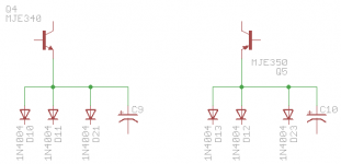
Looking at the photo you posted and comparing that to what I have, the difference is a 10R resistor in series with the emitter of Q4 and Q5 which are the MJE340/350 under the heat sinks. The catch is that the emitter Q4 is connected to the anodes of D10 & D11 (Q5 & D13 & D12 on the other side). Call this junction A. This junction is connected to the anode of D21 and positive end of C9 (D23 & C10 on the negative side) . Call this junction B. The 10R goes in between. I don't have an overlay for your PCB so you would need to work out where to cut the trace (and it is guaranteed to be under the PCB - Sod's law). So this may prove too difficult to perform.
Now to the power sensitivity setting for the APC board. There are 4 positions.
1 = 100W
2 = 200W
3 = 400W
4 = 800W
You can guess that the default factory setting would be position 4. I recommend position 1.
Alan,
I'll take a look at it. In order to remove the PCB, do I need to pull all the output devices, or can I get away with removing the screws and leaving them in place? If I need to remove the FETs, I'll need to pick up some heat sink compound. If removed, I assume short the gate to source pins, and put them in some antistat bags? And ensure that they go back in the same locations?
As for the power sensitivity setting, is this done via the set of stakepins with a jumper? And what are the 4 pots for?
Also, I emailed Mike regarding a Rev. B board or two, but he has not responded 🙂 I may call him if you think it would be worthwhile to have these (and the price isn't outrageous)... I would think he might have some around from upgrades.
Alan,
I'll take a look at it. In order to remove the PCB, do I need to pull all the output devices, or can I get away with removing the screws and leaving them in place?
Unfortunately, you need to remove the MOSFET to get at the rear of the PCB
If I need to remove the FETs, I'll need to pick up some heat sink compound
Yes. Even though these are probably silicon, rather than mica, insulators pads, they will still benefit from a smear of heat sink compound o either side of the insulator
If removed, I assume short the gate to source pins, and put them in some antistat bags?
All good practice.
And ensure that they go back in the same locations?
You just need to get the n and p channel devices in the same bank. They do not need to be in the exact same socket as before.
As for the power sensitivity setting, is this done via the set of stakepins with a jumper?
Yes
And what are the 4 pots for?
Various adjustments for the APC. Don't touch them!
I'm not sure that I would bother to get a new APC board. But I am recommending that you take some benefit from what you have.
Just so I am clear,Looking at the photo you posted and comparing that to what I have, the difference is a 10R resistor in series with the emitter of Q4 and Q5 which are the MJE340/350 under the heat sinks. The catch is that the emitter Q4 is connected to the anodes of D10 & D11 (Q5 & D13 & D12 on the other side). Call this junction A. This junction is connected to the anode of D21 and positive end of C9 (D23 & C10 on the negative side) . Call this junction B. The 10R goes in between. I don't have an overlay for your PCB so you would need to work out where to cut the trace (and it is guaranteed to be under the PCB - Sod's law). So this may prove too difficult to perform.
Now to the power sensitivity setting for the APC board. There are 4 positions.
1 = 100W
2 = 200W
3 = 400W
4 = 800W
You can guess that the default factory setting would be position 4. I recommend position 1.
- junction A above is the connection between the emitter of Q4 and the anodes of D10/11?
- junction B is the connection between the emitter of Q5 and D12/13?
- the traces to be cut are the junctions and the 10R are inserted here (one between Q4 emitter and the diodes, the other between Q5 emitter and diodes)?
Attachments
Last edited:
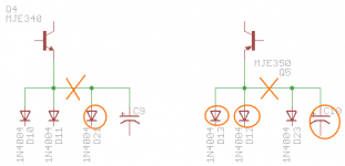
My apologies. My description had an error & was sloppy. See my version of your drawing. The circled components need to be reversed. The 'X' marks the point where the 10R resistors need to be inserted. D11 and D12 are 4.7V Zener diodes - 1N4732 which you may be able to read on the actual component.
Attachments
Thank Alan,
I spoke with my brother about this and he is leaving it up to me whether to do this or not. The prospect of damaging a good output device concerns me a bit. If I proceed, what would you recommend for heatsink paste, and should I use the probable mica insulators in there, or should I get something like the Bergquist line (digikey), such as these:
Digi-Key - BER100-ND (Manufacturer - SP600-05)
or these:
Digi-Key - BER152-ND (Manufacturer - SPK10-0.006-00-30)
I was considering using Arctic Silver paste, but it may be slightly conductive
Arctic Silver Incorporated - Arctic Silver 5
Or the Arctic Silver Ceramique, which apparently is not conductive:
Arctic Silver Incorporated - Céramique
I will try to get some antistatic foam from work to put the devices in/on while they are out. I also considered shorting the gate-source with a paper clip.
A good strategy is - if in doubt, don'tI spoke with my brother about this and he is leaving it up to me whether to do this or not. The prospect of damaging a good output device concerns me a bit
If I proceed, what would you recommend for heatsink paste, and should I use the probable mica insulators in there, or should I get something like the Bergquist line (digikey), such as these:
Digi-Key - BER100-ND (Manufacturer - SP600-05)
or these:
Digi-Key - BER152-ND (Manufacturer - SPK10-0.006-00-30)
If you disassemble carefully then you should be able to use the insulators that are already fitted. The only reason to change them is if you damage them.
Fancy paste is wasted. The silicon based insulators without paste are not quite as good as mica insulators plus paste, unless you pay for the very best. Mica has gone out of fashion because it requires paste, good technique and the mica will fracture if you are clumsy. In short, it was not tolerant of poor technique and so it went out of favour on production lines. My comment about using thermal compound on the silicon insulators is to squeeze the last drop of performance out of that technology and minimize the thermal resistance between the MOSFET and the heat sink.
Something like Digikey 473-1097-ND would do fine and not break the bank.
Just trying to evaluate the risk/reward aspect of doing this. It appears that Chris at least has never seen one fail in this manner; usually the outputs. I'm not sure if you have or not, but you came to the diagnosis pretty quickly (as in, immediately). My intuition is it is worth doing though the repaired channel is left unprotected. I suppose I could actually fix that board... maybe. It would be a bit of a challenge wiring the toasted pots in 🙄. Finding the two I/Cs could be fun as well.A good strategy is - if in doubt, don't
The SilPads dry may be a good alternative. Either the SP600 or SP400. The SP400 is a silicone/fiberglass construction which would hold up better perhaps for a TO-3 case.If you disassemble carefully then you should be able to use the insulators that are already fitted. The only reason to change them is if you damage them.
Fancy paste is wasted. The silicon based insulators without paste are not quite as good as mica insulators plus paste, unless you pay for the very best. Mica has gone out of fashion because it requires paste, good technique and the mica will fracture if you are clumsy. In short, it was not tolerant of poor technique and so it went out of favour on production lines. My comment about using thermal compound on the silicon insulators is to squeeze the last drop of performance out of that technology and minimize the thermal resistance between the MOSFET and the heat sink.
Something like Digikey 473-1097-ND would do fine and not break the bank.
If I decide to just stay with the mica (which I have some in TO-3 already), I can get the Arctic Silver Ceramique for ~$9 shipped (22g tube) which would be enough to do the whole amp. Non-conductive as well. Arctic Silver Incorporated - Céramique
A friend has offered a new thermal phase change product called UltraStick for the cost of shipping only; he has had very good results with this Interface Materials - Electrically Conductive - Thermal Greases
Last edited:
I made the suggestion before I realized how much work it would be. I thought it would be just a matter of lifting the transistor emitter leads and jamming the 10R in.Just trying to evaluate the risk/reward aspect of doing this
I suppose I could actually fix that board... maybe. It would be a bit of a challenge wiring the toasted pots in 🙄. Finding the two I/Cs could be fun as well.
I would not bother. That board is toast.
A friend has offered a new thermal phase change product called UltraStick for the cost of shipping only; he has had very good results with this Interface Materials - Electrically Conductive - Thermal Greases
Nope. If you look carefully, this stuff is expecting you to run the heat sink temperature up to 90 degrees Celsius, or at least well past 60 degrees Celsius. Not something I would recommend.
The paste or Silpads you mentioned above look good.
Alan,
I'm going to order some paste and then unbolt the heatsink and take a look at it. One thought I had was if I can locate the trace, I could possibly drill through it from the top and then solder the resistor from the one set of diodes to the other. Since this stuff is physically at the bottom of the board, it is hard to see right now, though I did find D10-13 and verified the anode connection (or whatever part I hit 🙂) to the emitters. I haven't located the other diodes/caps yet, but I'm sure they are right around there. The majority of the work, and all of the risk, seems to lie in the pulling and replacement of the FETs.
I'm going to order some paste and then unbolt the heatsink and take a look at it. One thought I had was if I can locate the trace, I could possibly drill through it from the top and then solder the resistor from the one set of diodes to the other. Since this stuff is physically at the bottom of the board, it is hard to see right now, though I did find D10-13 and verified the anode connection (or whatever part I hit 🙂) to the emitters. I haven't located the other diodes/caps yet, but I'm sure they are right around there. The majority of the work, and all of the risk, seems to lie in the pulling and replacement of the FETs.
Alan,
I unbolted the heatsink for the repaired channel tonight as it is easier to see these parts with Q4/Q5 removed in that channel (as well as a couple of the diodes in question).
I cannot find a D21 or D23. C9 and C10 are there (just below the neg. fuseholder, directly above Q4/Q5). The appropriate legs of C9/C10 ohm out to D10/11 and D12/13 top ends.
Since C9 and C10 are directly above the pads for the two transistors, it might be risky drilling holes blind hoping I take out the proper trace, unless I ohm out the base and collector of each to see if it is likely that their traces are routed in the same area (likely, but who knows). Since I don't know what is connected to them, ???
Since I can't find D21 or D23, could I lift the appropriate lead of these and solder the resistor in there? Or are other components also connected to the caps?
Chris
Here is a pic of this area on the repaired board.
If you can see the red and green lines I drew, those indicate the connections between the emitters and the diodes, and C9 and C10. I think I could lift the leads of C9/C10 and series the 10R here. Would I also need to add a diode for what you referred to as D21 and D23, and if so, what? From the "schematic" I drew up, I assume these would be in parallel with the caps?
I also assume that D21/D23 would not be soldered on the bottom of the board, across the caps (C9/C10)?
Does this, in combination with the 7815/7915, function as a Maida regulator or similar?
An externally hosted image should be here but it was not working when we last tested it.
If you can see the red and green lines I drew, those indicate the connections between the emitters and the diodes, and C9 and C10. I think I could lift the leads of C9/C10 and series the 10R here. Would I also need to add a diode for what you referred to as D21 and D23, and if so, what? From the "schematic" I drew up, I assume these would be in parallel with the caps?
I also assume that D21/D23 would not be soldered on the bottom of the board, across the caps (C9/C10)?
Does this, in combination with the 7815/7915, function as a Maida regulator or similar?
Last edited:
Nice work.Here is a pic of this area on the repaired board
I think I could lift the leads of C9/C10 and series the 10R here. Would I also need to add a diode for what you referred to as D21 and D23, and if so, what? From the "schematic" I drew up, I assume these would be in parallel with the caps? I also assume that D21/D23 would not be soldered on the bottom of the board, across the caps (C9/C10)?
Nope, I think you need to trace out the connections on one side. Work out what is connected (and where) to the base and emitter of Q4 and in/out of U5. Then i can figure out what the changes are. I think the difference is the addition of current limiting. Which would make sense.
Or similar, maybe, depending on your definition of similar...Does this, in combination with the 7815/7915, function as a Maida regulator or similar?
Here is what I find for the + reg section. Note that I can see two resistors on the back of the board (and those are the only components I can see on the back). They are down underneath the Q4/Q5 area. I am measuring ~91 ohms from the 7815 output to Q4 base, so I assume this is one of them. I can find no other components in this section of the board.
An externally hosted image should be here but it was not working when we last tested it.
Last edited:
That seems very wrong. Also if you look carefully at what you have drawn you will see that it will never work - not like this anyway.
Please check the connections to that 3k87 resistor. And what power rating is it? Is it a Roederstein MK3 (blue body) or something else. I think one end of the 3k87 and the collector of Q4 should connect to the +70V rail. And then the other end of the 3k87 should connect to the input of U5.
Now check D10 - are you sure that the cathode is connected to ground? I think it should go to the collector of Q4.
I'm trying to confirm what I think that original circuit is like. It may prove just too hard to hack into it to make a change. But let's not prejudge that issue.
Alan,
I will recheck tonight. D10 didn't make much sense that way, but that was what I was seeing. I had the meter in continuity mode rather than ohms much of the time. Will recheck in ohms mode.
From your post back on page 6 of this thread (?):
I also noticed in your first post you instructed me to remove R41/42, 10R resistors. These must be the ones we are trying to add?
I will recheck tonight. D10 didn't make much sense that way, but that was what I was seeing. I had the meter in continuity mode rather than ohms much of the time. Will recheck in ohms mode.
From your post back on page 6 of this thread (?):
1) You could if you like. If they are not dead now they soon will be but they are no longer connected to anything. Actually removing R34/R35 would be useful - that covers anything that might happen to the two 3-terminal regulators and they are easier to remove. They are 3k9 2W resistors found slightly above and between the two 15V regulators
I also noticed in your first post you instructed me to remove R41/42, 10R resistors. These must be the ones we are trying to add?
I also noticed in your first post you instructed me to remove R41/42, 10R resistors. These must be the ones we are trying to add?
Yes, and it looks like we need to add more bits.
- Home
- Amplifiers
- Solid State
- Counterpoint SA-220 problem...