You were, of course, correct 🙄
D10 goes from the emitter to the collector. R34 is in series with V+ to the regulator. The collector of Q4 comes straight from V+.
I attached the eagle schematic file I worked these up in as well.
D10 goes from the emitter to the collector. R34 is in series with V+ to the regulator. The collector of Q4 comes straight from V+.
An externally hosted image should be here but it was not working when we last tested it.
I attached the eagle schematic file I worked these up in as well.
Attachments
D10 goes from the emitter to the collector. R34 is in series with V+ to the regulator. The collector of Q4 comes straight from V+.
I'll redraw this so it makes more sense, Then show the mod required. Then you will need to figure out if that is achievable taking into consideration the amount of hacking needed
OK. I haven't pulled the output devices yet, otherwise this would have been easier if I had access to the bottom of the board.
I did get some heatsink compound, so I'm good there. I just looked and I don't have any mica pads, but do have some thermal TO-3 pads (NTE... yech). I can order some mica or good thermal pads (Bergquist) if I need them, otherwise I will reuse what is in there now.
I did get some heatsink compound, so I'm good there. I just looked and I don't have any mica pads, but do have some thermal TO-3 pads (NTE... yech). I can order some mica or good thermal pads (Bergquist) if I need them, otherwise I will reuse what is in there now.
The attachment shows the circuit that you have (the components inside the dotted box are replaced by shorts) and the later circuit, where the 'boxed' components are fitted.
I do not have a pcb overlay so I cannot assist in you with how this could be done.
I do not have a pcb overlay so I cannot assist in you with how this could be done.
Attachments
Alan,
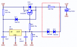
I would guess that C9 needs to stay in place if the 15V output comes off of it, so the trace between it and the anodes of D10/D11 would need to be cut. I'll need to check for an existing connection between the top junction of R36 and C9; if none, I can simply series the diodes between them. Otherwise, I'll need to cut that trace as well.
Are both D20 and D21 1N4148s? (D21 looks like 1N4140, or it is my eyes).
I hadn't mentioned that there are a pair of Wimas directly below Q4/Q5 and a pair of disc caps above the regulators; these are probably C4/C6 and the corresponding neg reg caps.
From what I have seen of CP service manuals, I'm surprised that you have a Rev. B schematic. I would guess you don't have the Rev. A one. Mike never got back to me regarding Rev. B boards, BTW. Not too surprising.
Thank you for all of your invaluable help! I know it is getting to be summer down there, and I'm sure you have much better things to do 🙂 I'll see how doable this is, and report back. My brother is fine with it the way it is, but avoiding another incident like he had with the L channel would be good.
EDIT: Also, R36 on my board measures ~4K5 or so. Does this need to be changed to a 10K? As I had mentioned, R41 measures around 91R, and is shown on your drawing as 100R. Change this as well?
Last edited:
Are both D20 and D21 1N4148s? (D21 looks like 1N4140, or it is my eyes).
Both are 1N4148. Blame it on my dodgy eyesight when it came to editing the png file which I extracted from my ECAD system
I hadn't mentioned that there are a pair of Wimas directly below Q4/Q5 and a pair of disc caps above the regulators; these are probably C4/C6 and the corresponding neg reg caps.
The WIMAs will be the 330nF and the ceramic disc caps will be the 100nF caps.
EDIT: Also, R36 on my board measures ~4K5 or so. Does this need to be changed to a 10K?
It is probably 4k7 which is a 3mA load on the 7815. Assuming that these are OnSemi parts, then regulation is specified for load currents > 5mA. So, leave it as it is. The active circuitry probably makes up the difference.
As I had mentioned, R41 measures around 91R, and is shown on your drawing as 100R. Change this as well?
This value is non-critical. Leave it as it is.
I assume that for the negative regulator section, the diodes all get reversed. Ohming the circuit out from R36 to C9 + leg is inconclusive; it ohms out at ~14K either way. Switching to diode mode, it shows a junction type reading one direction, and around 1.7V the other. Guess I'll have to look. I'll proceed if my brother wants me to, and you think it best.
I guessed on part numbers for the negative side.
An externally hosted image should be here but it was not working when we last tested it.
I guessed on part numbers for the negative side.
I assume that for the negative regulator section, the diodes all get reversed.
Your schematics look correct.
Ohming the circuit out from R36 to C9 + leg is inconclusive; it ohms out at ~14K either way. Switching to diode mode, it shows a junction type reading one direction, and around 1.7V the other
There may be residual damage. At least you now know what the final circuit should look like.
This was on the good channel, so there shouldn't be any damage. Looking at the schematic, I think this was the B-E junction of Q4 that I am seeing in diode mode. Red lead on R36 and black on C9 forward biases the junction (0.67V). Reversing leads, it shows 1.7V.
I also verified that the + side of C9 goes directly to the V+ pins on the ICs in the ACP (U3, U4, etc.). I'll probably proceed with this tomorrow night.
I also verified that the + side of C9 goes directly to the V+ pins on the ICs in the ACP (U3, U4, etc.). I'll probably proceed with this tomorrow night.
Pulled the output devices and went ahead and did the mods today. Still reinstalling the outputs, will let you know what happens when I fire it up 🙂
Here is a pic before I did anything. As you can see, the 91R resistors were themselves a factory mod. Must be part of the design by ear thing...
Traces cut, 10Rs installed. I decided it was easier to put these on the bottom.
Full mod complete. Used a bit of teflon tubing on the upper portions of the diode leads.
Here is a pic before I did anything. As you can see, the 91R resistors were themselves a factory mod. Must be part of the design by ear thing...
An externally hosted image should be here but it was not working when we last tested it.
Traces cut, 10Rs installed. I decided it was easier to put these on the bottom.
An externally hosted image should be here but it was not working when we last tested it.
Full mod complete. Used a bit of teflon tubing on the upper portions of the diode leads.
An externally hosted image should be here but it was not working when we last tested it.
Went ahead and fired it up, first on the variac so I could verify the +/- 15V supplies and make sure I didn't zap a FET. FETs were using mica and grease BTW, so just reused the mica with fresh grease (most of it).
Everything seems fine, including going straight from the wall. I'll run it a bit tomorrow to verify biasing (I hadn't run it much when I decreased the bias from 450 to 425mA). I'll run a signal thru it as well. Otherwise, I think it is good to go.
Thanks once again for all of your help Alan, and also Chris!
Thanks once again for all of your help Alan, and also Chris!
No problem. As you have no doubt gathered by now, the trick to working on these amps (indeed any high power amp) is not the minimal amount of actual work it takes to fix them but all the little hoops that you must jump through so that you don't damage what you have.
Hi Chris,
I'm just getting back now. Long time away.
I had no doubt that Alan would steer you down the right path. I'm very happy that you have the amp running. BTW, that modification was yet another piece of information we didn't receive from Counterpoint. Alan has been a wonderful source of information with this type for experience and information. Alan has supported this product line far better than Counterpoint has - sadly enough.
Alan, thank you very much!
-Chris
Good to see you back Chris. Hope you are doing OK (or better than OK).
Yes, I (and my brother) owe Alan a deep debt of gratitude for his assistance. The amp seems to be working fine and sounds just like he remembered it. Thanks for your help as well! Best wishes to you and Alan, and hope you have a Merry Christmas and Happy Holidays.
Yes, I (and my brother) owe Alan a deep debt of gratitude for his assistance. The amp seems to be working fine and sounds just like he remembered it. Thanks for your help as well! Best wishes to you and Alan, and hope you have a Merry Christmas and Happy Holidays.
Hi Chris,
Thank you.
Well, just enjoy that amp and don't leave it on all the time. The SA-100 in stock trim is unlistenable, so don't get any ideas about buying the little brother! I was extremely pleased that you have the amplifier running without having to attempt a matched set of outputs. Alan also gave you great advice. The factory limit setting is position 4 (useless as protection), but leaving it in the most sensitive position actually will allow that circuit to do something. Another over-complicated circuit to perform a rather simple task. Oh well.
Enjoy your holidays and Merry Christmas!
-Chris
Hi Alan and Chris,
Well, it's back...
My brother sent an email/photo and dropped the amp off. The previously good channel is blowing both rail fuses (6A). He replaced them and they both blew again (immediately). Speaker fuse did not blow. He ohmed out the speaker cable on that side, and swapped it to the previously-repaired channel and it works fine.
Any thoughts before I dig into this side? Q1 looks a bit toasty but otherwise I don't see anything. I'm thinking the output devices may be toast on this side...
An externally hosted image should be here but it was not working when we last tested it.
🙁 You are a seasoned campaigner by now. You know what to do. Progress slowly, steadily and methodically.
Heh. I'm glad you think so. 🙄
Since I don't have schematics for this I was just wondering if there was something other than a blown output device that would cause both +/-70V rail fuses to blow. Ohming out the output shows ~370ohms steady vs. megohms for the working channel. Ohming out the bridging strips to one another it would appear that the front bank (P channel devices) has a problem.
I'll look into it some more; have not had more than a few minutes to spend on this so far. Q1 seems to be fine, though it does look like it has gotten hot. Not sure what it's function is though.
Last edited:
Took a brief look at this tonight. The gate resistors appear to be fine, as well as the protection zeners. Interestingly, when I removed the input relay on the bad channel, the output resistance went from 370 ohms up to 25K ohms. Doing the same on the good channel had no effect, output resistance stayed at 3.7M ohms or so. Flipping lead polarity made no difference on either channel.
The poster on the first page of the thread that had an SA-20 with one good channel and had offered the MOSFETs and output board has already given it away, so no joy there. I still think it is a bad FET or more, so I think I will start pulling FETs one by one and see what happens on the output resistance.
The poster on the first page of the thread that had an SA-20 with one good channel and had offered the MOSFETs and output board has already given it away, so no joy there. I still think it is a bad FET or more, so I think I will start pulling FETs one by one and see what happens on the output resistance.
Took a more detailed look tonight. Doing a simple DMM test on removed devices, it appears that 1 P ch and 2 N ch devices are bad. Since the gentleman on the first page of this thread no longer has the good SA20 channel and devices, guess it is new amp time, unless my brother can find another donor amp. MElliot is charging $360 or something like that for a set of output devices. Don't think so.
One thought would be to try it with half of the output devices (probably at reduced power). Since the devices are in parallel, I would think it would work (sorta).
One thought would be to try it with half of the output devices (probably at reduced power). Since the devices are in parallel, I would think it would work (sorta).
Last edited:
- Home
- Amplifiers
- Solid State
- Counterpoint SA-220 problem...