Give us the pdf for home etching.🙂OK, here comes the layout...
8.5 x 3 inch, double-sided. Not really simple any more 🙂
However - still pretty cool 😉
Placing the order tomorrow... takes about a week to produce.
And then we'll see...
P.S. Big ones are actually under the board - 3D renderer just can't show them the right way 🙂 Anyway, gives an impression.

PDFs
Hi Thimios,
Here go the PDFs in the following order:
1) Top traces;
2) Bottom traces;
3) Top silk.
I did not mirror anything, so let me know is you need more "views" 😉
Cheers,
Valery
Hi Thimios,
Here go the PDFs in the following order:
1) Top traces;
2) Bottom traces;
3) Top silk.
I did not mirror anything, so let me know is you need more "views" 😉
Cheers,
Valery
Attachments
Ok i believe that is all i need,just post the schematic according to this.🙂Hi Thimios,
Here go the PDFs in the following order:
1) Top traces;
2) Bottom traces;
3) Top silk.
I did not mirror anything, so let me know is you need more "views" 😉
Cheers,
Valery
PS is this according to post#21?
Thanks again.
Thimios.
Last edited:
Is this one safe to run at a little higher voltage rails or is 52 around it's limit? Looks like a fun project!
Ok i believe that is all i need,just post the schematic according to this.🙂
PS is this according to post#21?
Thanks again.
Thimios.
No, this one is exactly per post #37
Cheers,
Valery
Is this one safe to run at a little higher voltage rails or is 52 around it's limit? Looks like a fun project!
No, it's not the limit - I will actually run it at around 52-56 (got a couple of 1KW transformers 😉), but it can be higher.
Let me know, how much you need - I will check if some adjustments are needed.
I have a 63 volt supply to test with. I might make up a lower voltage one but I prefer higher voltage amps.
Just a suggestion here but you've got a wonderful protection system designed. Ever thought of adding a couple pads to connect your overcurrent sensing?😉
Just a suggestion here but you've got a wonderful protection system designed. Ever thought of adding a couple pads to connect your overcurrent sensing?😉
OK, just checked the parameters, for 63V rails:
R5, R8 = 63K
R38, R39 = 8.2K
All the rest is perfectly fine - no adjustments required.
Overcurrrent sensing - you're right, however, the PCB is rather packed. In a few other designs I just soldered a 2-pin plug right on top of the big resistors 🙂
Although, I will think where to place it in the refined version of the PCB...
OK, just checked the parameters, for 63V rails:
R5, R8 = 63K
R38, R39 = 8.2K
All the rest is perfectly fine - no adjustments required.
Overcurrrent sensing - you're right, however, the PCB is rather packed. In a few other designs I just soldered a 2-pin plug right on top of the big resistors 🙂
Although, I will think where to place it in the refined version of the PCB...
Yes that board does look kind of full. Thanks.
Thimios, wait! Jeff's question has inspired one good idea 🙂 I wanted to avoid CCSs for the input pair, but using them will make the amp more tolerant to the rails variation / fluctuation. I have found an elegant way of implementing them.
Schematic and PCB will be slightly updated! 😉
Schematic and PCB will be slightly updated! 😉
Just a very little bit less (6 parts added). But now it's virtually rail voltage independent 😉
At least in the range +/-45V to +/-70V no adjustments required.
It's also more tolerant to rail "sagging" caused by high power consumption or mains fluctuations
At least in the range +/-45V to +/-70V no adjustments required.
It's also more tolerant to rail "sagging" caused by high power consumption or mains fluctuations
Last edited:
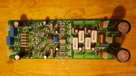
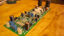
Version 02
Here goes v02.
I have also added the "BIAS" plug for overcurrent sensor - in the middle of PCB. Size is the same, just "cleaned up" some space 🙂
Have fun!
Here goes v02.
I have also added the "BIAS" plug for overcurrent sensor - in the middle of PCB. Size is the same, just "cleaned up" some space 🙂
Have fun!
Attachments
-
03-CFA-CFP-02-PCB-Silk.pdf108.2 KB · Views: 232
-
02-CFA-CFP-02-PCB-Bot.pdf60.5 KB · Views: 181
-
01-CFA-CFP-02-PCB-Top.pdf59.9 KB · Views: 202
-
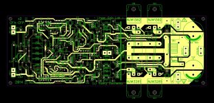 @04-CFA-CFP-02-pcb-traces.JPG287.4 KB · Views: 830
 -
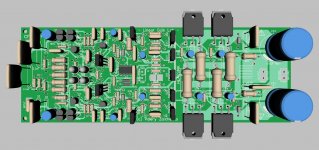 @03-CFA-CFP-02-pcb-3D.JPG196.1 KB · Views: 845
 -
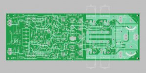 @02-CFA-CFP-02-pcb-silk.JPG187.7 KB · Views: 910
 -
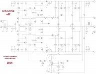 @01-CFA-CFP-02-sch.jpg405.8 KB · Views: 956
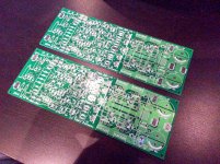
Has anyone tested this amp?
Hi Jeff,
I have just received the PCBs - 3 minutes ago 🙂 I believe I will be the first to try 😉
Cheers,
Valery
Attachments
- Status
- Not open for further replies.
- Home
- Amplifiers
- Solid State
- Cool simple "clean" CFA