Hi valery, what is open loop gain and bandwith from the latest schematic post#126??
Do you else have any news / thoughts regarding this amplifier?
Hi kimschips,
I will try to access one of my home servers later today - as I'm living on the mountain these days, my access to information is a bit limited. But still possible 🙂
I will show you the curves.
Cheers,
Valery
Hi guys have you any news here?
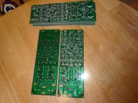
I've got a single-channel prototype running now, ordered two more PCBs to buyld a stereo amp in a nice compartment.
I've got a single BJT board up and running. I'm having very similar DC offset issues like I was with the Tubesomo boards for the last couple days. I'm really starting to wonder about this batch of op amps.
Curves are nice🙂- are you on vacation?
Thanks Valery🙂
Yes, I'm on vacation in Swiss Alps - skiing and relaxing 🙂
Hi Jeff, interesting - I didn't notice this specialty with regards to input cabling. Maybe I just had the right cabling all the time - I don't know 🙂
For BJT outputs, you need:
Q18, Q22 = NJW1302
Q19, Q23 = NJW3281
R42, R43, R52, R53 = 100R
R44, R45, R54, R55 = 2.2R
No PCB changes required - which is pretty cool 🙂
Do any of you know if I can use MJL4302 / MJL4281 instead of NJ1302 / NJW3281?
Man, do you do anything that isn't fun?
Terry, I'm trying to keep it this way 🙂 Not always possible, but most of the time I succeed 😛
Fun and challenge

Do any of you know if I can use MJL4302 / MJL4281 instead of NJ1302 / NJW3281?
From what I see in the datasheet - should be ok.
Curves are nice🙂- are you on vacation?
Thanks Valery🙂
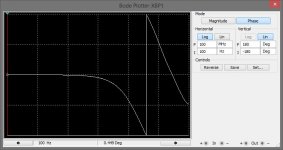
OK, I have finally reached my server remotely and have built the curves.
They are pretty "clean", as promised in the thread title 🙂)), showing the following key parameters (rounded values):
ULGF: 1MHz
Phase Margin: 84 degrees
Gain Margin: 20db
CLG: 29db (set by global NFB)
OLG(1KHz): 57db
LG(1KHz): 28db
OLG(20KHz): 35db
LG(20KHz): 6db
In overall, this is a rather low LG, high-linearity design.
Cheers,
Valery
Attachments
Here goes a simple one! 🙂
Ready for something new? 😉
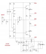
Greetings from Switzerland, I'm still here. Skiing was limited during the last couple of days due to avalanche danger - no problem, spare time was used for testing some front-end ideas 😛
Of course, not prototyped yet - I will work on PCB over the weekend - however it is simmed thoroughly and looks very promising.
Only 8 active devices (excluding DC servo). Compensation - single lead cap. All the rest is done by the FETs' internal capacitance. Very simple. DIYer's dream 😀
JFET input stage, JFET-MOSFET "super-pair" VAS stage. That's basically it. Two BGTs are used as a cascode (common base) for limiting the input JFETs drain voltage.
Developing this front-end, I actually had in mind my simple Lateral-FET OPS from TubSuMo project. Partially for that purpose, VAS is running at high current (20mA). If somebody wants to use it together with other OPS modules, designed for lower VAS currents (4-5 mA) - no problem, one can change R1, R3 to 43R. Similar performance with probably very slightly higher THD at 10-20KHz.
Attached files represent:
1) Front-end schematic;
2) Front-end together with Lateral-FET OPS (all further measurements are done for this particular combination);
3) Clipping behavior - nice, soft, rounded corners;
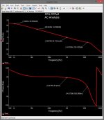
4) Closed loop frequency response (left edge is 100 Hz);
5) Closed loop phase response (left edge is 100 Hz);
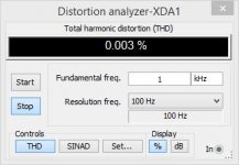
6) THD @ 1KHz (simulated value);
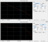
7) AC analysis - Phase Margin;
8) AC analysis - Gain Margin.
Key parameters (so far - per simulation):
Output power - up to around 120W @ 8R (with +/-52V rails);
Voltage gain: 29db;
ULGF = 1.625MHz;
Phase margin: 86.5 degrees;
Gain margin: 26db;
THD @ 1W: 1KHz<0.001%; 10KHz=0.002%; 20KHz=0.006%;
THD @ 50W: 1KHz=0.003%; 10KHz=0.016%; 20KHz=0.038%;
Pretty cool, especially at lower volumes. Would be interesting to audition.
All for now, have fun, stay tuned - further development will follow 😉
Cheers,
Valery
Ready for something new? 😉
Greetings from Switzerland, I'm still here. Skiing was limited during the last couple of days due to avalanche danger - no problem, spare time was used for testing some front-end ideas 😛
Of course, not prototyped yet - I will work on PCB over the weekend - however it is simmed thoroughly and looks very promising.
Only 8 active devices (excluding DC servo). Compensation - single lead cap. All the rest is done by the FETs' internal capacitance. Very simple. DIYer's dream 😀
JFET input stage, JFET-MOSFET "super-pair" VAS stage. That's basically it. Two BGTs are used as a cascode (common base) for limiting the input JFETs drain voltage.
Developing this front-end, I actually had in mind my simple Lateral-FET OPS from TubSuMo project. Partially for that purpose, VAS is running at high current (20mA). If somebody wants to use it together with other OPS modules, designed for lower VAS currents (4-5 mA) - no problem, one can change R1, R3 to 43R. Similar performance with probably very slightly higher THD at 10-20KHz.
Attached files represent:
1) Front-end schematic;
2) Front-end together with Lateral-FET OPS (all further measurements are done for this particular combination);
3) Clipping behavior - nice, soft, rounded corners;
4) Closed loop frequency response (left edge is 100 Hz);
5) Closed loop phase response (left edge is 100 Hz);
6) THD @ 1KHz (simulated value);
7) AC analysis - Phase Margin;
8) AC analysis - Gain Margin.
Key parameters (so far - per simulation):
Output power - up to around 120W @ 8R (with +/-52V rails);
Voltage gain: 29db;
ULGF = 1.625MHz;
Phase margin: 86.5 degrees;
Gain margin: 26db;
THD @ 1W: 1KHz<0.001%; 10KHz=0.002%; 20KHz=0.006%;
THD @ 50W: 1KHz=0.003%; 10KHz=0.016%; 20KHz=0.038%;
Pretty cool, especially at lower volumes. Would be interesting to audition.
All for now, have fun, stay tuned - further development will follow 😉
Cheers,
Valery
Attachments
-
 z01-Phase-Margin.JPG84.2 KB · Views: 158
 -
 THD-01K.JPG23.9 KB · Views: 154
 -
 Phase-Responce.JPG51.3 KB · Views: 148
 -
 Frequency-Responce.JPG49.6 KB · Views: 443
 -
 Clipping.JPG63.8 KB · Views: 575
 -
 02-CF-FET-Sch-Full.jpg200 KB · Views: 620
 -
 01-CF-FET-Sch-IPS.jpg125 KB · Views: 619
 -
 z02-Gain-Margin.JPG84 KB · Views: 163
Already ordered some in Moscow store 😉
Renesas laterals seem to be more difficult there, as they stock them in small volumes. So I order 4-6 pieces from time to time just to maintain my own stockpile 🙂
Renesas laterals seem to be more difficult there, as they stock them in small volumes. So I order 4-6 pieces from time to time just to maintain my own stockpile 🙂
Already ordered some in Moscow store 😉
Renesas laterals seem to be more difficult there, as they stock them in small volumes. So I order 4-6 pieces from time to time just to maintain my own stockpile 🙂
I got a tip on lsk117s today so I bought 100 of them. These small signal fets are tough to find.
I got a tip on lsk117s today so I bought 100 of them. These small signal fets are tough to find.
I like the approach
It's a good low-noise jfet. Great for inputs.I like the approach
I've been trying to find them since you came up with the compact cfa. Tayda sold out the next day before I could order any.
Ready for something new? 😉
Greetings from Switzerland, I'm still here. Skiing was limited during the last couple of days due to avalanche danger - no problem, spare time was used for testing some front-end ideas 😛
Of course, not prototyped yet - I will work on PCB over the weekend - however it is simmed thoroughly and looks very promising.
Only 8 active devices (excluding DC servo). Compensation - single lead cap. All the rest is done by the FETs' internal capacitance. Very simple. DIYer's dream 😀
JFET input stage, JFET-MOSFET "super-pair" VAS stage. That's basically it. Two BGTs are used as a cascode (common base) for limiting the input JFETs drain voltage.
Developing this front-end, I actually had in mind my simple Lateral-FET OPS from TubSuMo project. Partially for that purpose, VAS is running at high current (20mA). If somebody wants to use it together with other OPS modules, designed for lower VAS currents (4-5 mA) - no problem, one can change R1, R3 to 43R. Similar performance with probably very slightly higher THD at 10-20KHz.
Attached files represent:
1) Front-end schematic;
2) Front-end together with Lateral-FET OPS (all further measurements are done for this particular combination);
3) Clipping behavior - nice, soft, rounded corners;
4) Closed loop frequency response (left edge is 100 Hz);
5) Closed loop phase response (left edge is 100 Hz);
6) THD @ 1KHz (simulated value);
7) AC analysis - Phase Margin;
8) AC analysis - Gain Margin.
Key parameters (so far - per simulation):
Output power - up to around 120W @ 8R (with +/-52V rails);
Voltage gain: 29db;
ULGF = 1.625MHz;
Phase margin: 86.5 degrees;
Gain margin: 26db;
THD @ 1W: 1KHz<0.001%; 10KHz=0.002%; 20KHz=0.006%;
THD @ 50W: 1KHz=0.003%; 10KHz=0.016%; 20KHz=0.038%;
Pretty cool, especially at lower volumes. Would be interesting to audition.
All for now, have fun, stay tuned - further development will follow 😉
Cheers,
Valery
Hi Valery! FYI -- this is exactly the topolgoy I use for almost 40 years now.
😎🙂
THx-RNMarsh
I like the approach
This one fits the title of the thread a little better. 😀
Can this one be tailored to work with the Slewmaster OPS as well?
Blessings, Terry
Hi Valery! FYI -- this is exactly the topolgoy I use for almost 40 years now.
😎🙂
THx-RNMarsh
Hi Richard - it's not so new then 😀 But it makes me sure I'm going in the right direction 🙂
Cheers,
Valery
- Status
- Not open for further replies.
- Home
- Amplifiers
- Solid State
- Cool simple "clean" CFA