With this kind of bias tracking I would strongly recommend minimum 220 nF from base Q14 to base Q15.
Also, base stoppers Q16-19, 10R or more, would be advisable 🙂
Tried a 470nF cap between base of Q15 and Q14, no effect. Maybe I'll try with base stopper tomorrow, it's a little trickier to do.
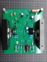
Can you post a photo of the thing? The way you wire it and the layout can have as much impact as component values. When touching heatsinks causes oscillations you know you are in serious trouble.
A stable amp does not get excited when you touch metalwork or put your hand near to circuitry. And a stable amp's output, with no input connected, should have no mains hum at all; a connected speaker should be silent even with your ear right against it.
I think the schematic circuit is iffy, but I wonder whether you have issues due to the build?
Just give up any CFP design. Problem solved.
The "faster" scam of any CFP advantages are far outweighed by the EF3. EF3/EF2 has been perfected in this community.
The "faster" scam of any CFP advantages are far outweighed by the EF3. EF3/EF2 has been perfected in this community.

Sure, here's a pic of the finished amp and the Gerber files if your interested.Can you post a photo of the thing? The way you wire it and the layout can have as much impact as component values. When touching heatsinks causes oscillations you know you are in serious trouble.
Yeah that was my thought too. Therefor I picked values of the degen resistors and compensating cap, then this did not occur. My very nonscientific measurement of a "stable amp".A stable amp does not get excited when you touch metalwork or put your hand near to circuitry. And a stable amp's output, with no input connected, should have no mains hum at all; a connected speaker should be silent even with your ear right against it.
I think the schematic circuit is iffy, but I wonder whether you have issues due to the build?
I'm very aware of that poor design can lead to issues like this. And therefore I used the exact layout as for fig 6.11 in Randy Slone's book "The Audiophile's Project Source book" (except that I substituted the jumpers with layer 2). That amp is a much bigger amp, but the schematic is almost the same, except for the components values and the bigger amp also involves a tho pole compensating capacitor network for the VAS. That's why you see some jumpers instead of resistors and capacitors at my board. This is also why the legs are twisted of some of the 2N3904/06, the bigger version uses 2SB649/2SD669 here instead which are ECB devices.
As I said before my plan was to build this smaller version of the amp first, too see I can get it working before trying the bigger version. The cost is of course much higher, MJ15004/03 devices are around 10 dollar a piece, compared to TIP32 maybe one dollar.
Think I read in the foreword of Randy Slone's book that hi guarantees that all his includes designs actually worked as promised... well I'm getting some doubts now, but not giving up yet.
Attachments
I have been watching this thread with interest.
I agree with ostripper that the emitter-follower is much more stable.
The CFP has voltage gain in its feedback loop, but because both the driver and output transistors operate in class AB, the gain varies widely.
The CFP may be salvageable by adding small emitter resistors to the driver transistors to reduce the loop gain. Try 10-20 ohms. These resistors will also negate the distortion benefits.
Ed
Well I'm not ready to completely give up the CFP design yet, even though I see the downsides with it now.
Adding emitter resistors to the driver transistor was a new idea. And this would help with oscillation by reducing the local feedback gain of the driver/output transistors (?)
However the amp is stable now after the changes I made. Not sure if this was how it was intended to work in the first place, and nor have I made any THD measurements yet. So far @WhiteDragon 's explanation makes sense, compared to my tests. I found it hard to believe the desing would be totalty wrong in the first place, since it from a well recognized author. If the original problem only lies in the components wvles it makes more sense, maybe un typing error in the original schematic in the book?
Next I was thinking about substituting the output devices to something with higher gain bandwidth and see if it improves anything. I guess Slone just used TIP32/31 couase he had them or smoehitng maybe.
Depends what voltage you plan on running the amp at.
This pretty straight forward input topology.
Once you add a mirror to the differential and drive 2nd gain stage
with beta enhancement.
1st gain stage will be rather picky with current.
Slew rate would technically improve with high current
at 2ma or 3ma. But it will make the amp oscillate
Typically current needs to be 1 to 1.5 ma. and no more.
Add a CFP output and you riding the edge of a knife.
Basically the initial problem. was DC offset
once the current sources were dialed in
the amp stabilized.
And depending on the exact voltage being used for rails.
Basically everything could be dialed in.
With Darlington amps people run 2nd stage or Q11
rather hot at 8 to 10ma.
With CFP bias will be jumpy that hot.
And the single drop of the drivers justify how bias behaves.
So CFP amps are very very picky with DC current of every single
stage. 6ma is ok for second gain stage, and drivers need 3ma
for every output device driven, no less no more.
need to know exact rail voltages then the overall DC
of the amp could be dialed in to perfection.
No wild guessing. 1st stage, mirror, beta enhancement, drivers
everything needs to be specific for thermal stability and feedback
stability.
Long story short, CFP has been abandoned for many of these
reasons.
Even when you dial them in with best devices possible.
THD at high frequency is always poop. Most of Elliots
rantings about superiority can be ignored. rather quickly.
Funniest thing to do with CFP is add feedback to the output stage.
Watch everyone freak out. Using Mosfets which are fast enough.
You can overcome the huge 4 to 6 volt losses typically found with
mosfets.
Can I assume your sig gnd and speaker gnd are not connected on the PCB, and they are connected at a single star point at the psu?
I don't like the distance on the pcb between Q3 base and R11 and R12. The base of Q3 is extremely sensitive...any noise there gets amplified by the full open loop gain. The copper traces attached to Q3 should be as short as possible.
C3 is too far from Q2. The purpose of C3 is to AC ground Q2 base at HF.
And then C8 is sort of out there on its own.
No point going any further. Too many layout provocations for instability for me. Is this the same component spacing in Randy Slone's layout?
I would assume that the oscillation is created in the CFP output stage.
Try putting a 22R in the emitter of the small CFP transistor (the driver).
HD
Try putting a 22R in the emitter of the small CFP transistor (the driver).
HD
Depends what voltage you plan on running the amp at.
This pretty straight forward input topology.
Once you add a mirror to the differential and drive 2nd gain stage
with beta enhancement.
1st gain stage will be rather picky with current.
Slew rate would technically improve with high current
at 2ma or 3ma. But it will make the amp oscillate
Typically current needs to be 1 to 1.5 ma. and no more.
Add a CFP output and you riding the edge of a knife.
Well at least for now I plan to run it at +/-15 V, which gives me 12 W rms into 8 ohm, which was the design goal of this amp by the Slone. I assume you mean the input stage (differential amp and current mirror) with first gain stage?
Current to the differential pair is set by R3, now 120 which gives a current of 5,6 mA (0,67/R3). Before it was 4,5 mA but I increased it because I increased the the compensating cap, then alse increasing the current need of the VAS. Or are we taking about the same thing? (I did substitute R3 with a pot for a while, controlling it between 100 - 500 ohms, and it didn't have a significant effect of the amp. Too low however decreased slew rate, as expected.)
Basically the initial problem. was DC offset
once the current sources were dialed in
the amp stabilized.
And depending on the exact voltage being used for rails.
Basically everything could be dialed in.
With Darlington amps people run 2nd stage or Q11
rather hot at 8 to 10ma.
With CFP bias will be jumpy that hot.
And the single drop of the drivers justify how bias behaves.
So CFP amps are very very picky with DC current of every single
stage. 6ma is ok for second gain stage, and drivers need 3ma
for every output device driven, no less no more.
Please explain this, the 2nd stage is indeed a dralington VAS yes. But witch current is of interest, current through Q11? I've done a lot reading trying to figure this out. The Darlington VAS need a constant current source, which I believe is made of Q8 using the reference voltage from the input stage constant current source. I measure about 13,7 V at base of Q8, so with R14 at 100 ohm this should yield approx 13 mA (?) This is quite "hot" if we're taking about the same thing.
need to know exact rail voltages then the overall DC
of the amp could be dialed in to perfection.
No wild guessing. 1st stage, mirror, beta enhancement, drivers
everything needs to be specific for thermal stability and feedback
stability.
If you interesteing I'll glaldy post a schematic with some voltage readings. This has been very educational form me, really appreciate it.
Yes signal GND and speaker GND are both connected to the PSU GND at a starpoint.Can I assume your sig gnd and speaker gnd are not connected on the PCB, and they are connected at a single star point at the psu?
I don't like the distance on the pcb between Q3 base and R11 and R12. The base of Q3 is extremely sensitive...any noise there gets amplified by the full open loop gain. The copper traces attached to Q3 should be as short as possible.
C3 is too far from Q2. The purpose of C3 is to AC ground Q2 base at HF.
And then C8 is sort of out there on its own.
No point going any further. Too many layout provocations for instability for me. Is this the same component spacing in Randy Slone's layout?
Isn't C3 a lowpass filter just in combination with R1?
I can agree that there are some questionable things about the design. But yes, it is very identical, also in scale including component spacing to the layout from his book "The Audiophile's Project Sourcebook" (don't want to post it here for to copy right reasons). The design in his book was makde for single PCB, and using DIY methods for manufacturing. Which may explain the very generous spacing and so on. But I thought his the expert so made an order for 5 pcs to try it. There are some things i may change if I go furhter with this design thoug. Traces around Q3 may be a good idea.
Then I build the next board for the other channel I'll try this, hard to get into the board right now.Try putting a 22R in the emitter of the small CFP transistor (the driver).
Well observed! Must have been some bad test probes or mistake by me. Corrected now.
Read in some book that CF output stages bias can be set by measuring 8 mV across both collecter resistors (R33 and R34). But isntead I'd just adjusted it so I had 1,29 volts across bias transistors Q9 isntead, as suggested by Slone.
Read in some book that CF output stages bias can be set by measuring 8 mV across both collecter resistors (R33 and R34). But isntead I'd just adjusted it so I had 1,29 volts across bias transistors Q9 isntead, as suggested by Slone.
Attachments
your looking for the common 30ma current per device and their is a pair so 60ma total.
8 mV across R33/34 if .22 ohm around 35ma, so is a good starting point if amp was cold.
or a low bias setting to be conservative and observe the amp.
Otherwise if at temp and reasonable stabilized thermally.
60ma total be around 13 mV drop across r33 or r34
and it could climb as high as 16 mV
basically if amp is hot and running 13 to 15mV
tells you around 60 to 65 ma
and its starting to creep into 70 to 85 ma
18 to 20 mV
this board design for running multiple CFP output transistors
has been done close to " proper" for thermal stability and
current sharing. since CFP has slight amount feedback.
extra resistors are needed
so technically Degen is also added to the drivers.
when running multiple outputs.
but this board has no degen on drivers
Correct value depends on driver transistor used.
and overall DC current needed to still be 5 to 6ma for CFP
driving 2 output devices.
usually with 100 ohms on driver collectors.
6.8 to 10 ohms be fine for degen on driver emitters.
R1-C3 act as a LPF for the input signal, but that's not the only purpose of C3. And, as was mentioned earlier, C3 should be a lot larger...like 500pF, and R1 should be 10x as big, like 1.5k. Slone didn't think this through.Isn't C3 a lowpass filter just in combination with R1?
@traderbamIf you want exact value 150 ohms would need 353p for 3MHz
and 330p or 470p standard values be more than fine.
Hardly doubt radio is getting in so the current values more than fine
Far as RF for lower AM bands 3 MHz all you worry about. you can take it down too 1.5 MHz to feel better
R1 is typical 1k so
fc= 1/(2πRC).
3 MHz R1 = 1k C3 = 53p
So standard value 56p be more than fine
3MHz R1 = 150 ohms C3 = 353p
330p or 470p more than fine.
Real life even without a resistor, just having 47 to 100p
on the input usually kills RF.
Well here's my DC voltages if anyone still is interested. Measured after 30 min with no input or output connected.
Looking at the current of first gain stage set by Q1 current source and R3 =120R
First gain stage is rather hot around 5.6 ma.
And would expect the mirror to be helping maintain DC offset.
But the amp would likely have negative offset.
looking at output , is just that =negative
looks respectable less than 1 mv. but that is because
the mirror is helping and fighting excess offset.
As mentioned Differential stage, with current mirror
feeding 2nd stage with beta enhancement. If first gain stage
is more than 3ma then distortion might read low. But the amp can
be rather touchy for stability.
Driving beta enhancement 2nd gain stage.
1st stage should be no more than 1.5 to 2 ma.
Anyhoo ..raise R3 to 330 ohms and 1st stage will be proper 2ma
the amp could likely be more stable, might reduce Cdom lower than 100p.
Even if it doesnt.
DC offset should be positive. For non inventing amplifier
Most would ignore it, since mirrors keep offset respectable.
1 mv is fine...But if I see a non inverting amp with negative offset.
Just tells me there is too much current somewhere.
This case 5.6ma for 1st stage is way too hot.
Today I finished building another identical board for the other channel. Having the opportunity to have to identical boards to compare I started to do some experimenting. First I tried some different combination of emitter resistors for the drivers, none of it had any effect. Maybe a little worse actually with 10 emitter resistors.
Nor had I any luck with two pole compensating capacitor networks. Nothing I do, except for increasing the degen resistors in input-stage apperad to have any real effect at stability. And any lower value of compensating capacitor C8 than 100 pF was still not possible.
However, you were right again @WhiteDragon about R3. I selected the value 120 ohm after reading Randy Slones book "High Power ampifier construction manual", a great book were the compensating cap and current of input stage is described in detail. And after som calcualations came up with that the current should be around 4-5 mA. But I noticed that the amp with 120 ohm for R3 (wich was the only different at this point) had - 1 mV offset at the output and the other one with 330 ohm for R3 had +1 mV. As you sad, it should be positive.
Also I could here this hissing noise again from the board with the negative offset, and located the source of it the heatsink of one of the driver transitros Q15. So after some probing around, I found this at the driver transistor emiiters;

This is at Q15, channel 1 has R3=330, channel R3=120 ohm.

This is at Q8, channel 1 has R3=330, channel R3=120 ohm.
After changing to 330 ohm for R3, this disappeared and offset was +1mV at both boards. Compared to the one with 120 ohm, the slew rate was not decreased very much that I could se (which could be the downside of too small current for input stage according to Slone). Here's the response for 20khz square wave, channel 1 has R3=330, channel R3=120 ohm.

After all this tweaking with components values, I believe that I've found some middle ground that actually works. Changing some values instead of trowing in a lot of capacitor makes more sense to me. It still bothers me that it didn't worked from the start as Slone guaranteed that it would. Maybe he got sloppy and copied some component values from other designs, or printing error. I'll never know probably. Thanks for all the support, I learned a lot of this.
Nor had I any luck with two pole compensating capacitor networks. Nothing I do, except for increasing the degen resistors in input-stage apperad to have any real effect at stability. And any lower value of compensating capacitor C8 than 100 pF was still not possible.
However, you were right again @WhiteDragon about R3. I selected the value 120 ohm after reading Randy Slones book "High Power ampifier construction manual", a great book were the compensating cap and current of input stage is described in detail. And after som calcualations came up with that the current should be around 4-5 mA. But I noticed that the amp with 120 ohm for R3 (wich was the only different at this point) had - 1 mV offset at the output and the other one with 330 ohm for R3 had +1 mV. As you sad, it should be positive.
Also I could here this hissing noise again from the board with the negative offset, and located the source of it the heatsink of one of the driver transitros Q15. So after some probing around, I found this at the driver transistor emiiters;
This is at Q15, channel 1 has R3=330, channel R3=120 ohm.
This is at Q8, channel 1 has R3=330, channel R3=120 ohm.
After changing to 330 ohm for R3, this disappeared and offset was +1mV at both boards. Compared to the one with 120 ohm, the slew rate was not decreased very much that I could se (which could be the downside of too small current for input stage according to Slone). Here's the response for 20khz square wave, channel 1 has R3=330, channel R3=120 ohm.
After all this tweaking with components values, I believe that I've found some middle ground that actually works. Changing some values instead of trowing in a lot of capacitor makes more sense to me. It still bothers me that it didn't worked from the start as Slone guaranteed that it would. Maybe he got sloppy and copied some component values from other designs, or printing error. I'll never know probably. Thanks for all the support, I learned a lot of this.
- Home
- Amplifiers
- Solid State
- Complementary Feedback design amp oscillating problems