811 is the mono version of 4702 with slight layout changes. 830 is specifically designed to drive mosfet output stages. 810 is beefed up version of 811 but having a classAB driver stage (811 has class A stage) to deliver extra current and has some extra features like baker clamp . You can consider that 810 is designed for hall and concert audio reproduction systems and 811 for hifi systems. You can find comments of Audioman54, a former National employee, in forum regarding these chips.
I did aural comparison with all the above chips and all of them sound different and I have read many of the audioman54 mark`s threads and replies. Agreed but my question is that if LM4702 can drive mosfets then can 811? can drive? or TI ripped off the higher Vbias feature in 811?
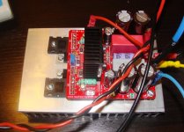
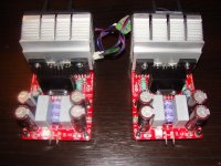
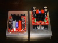
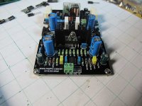
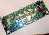
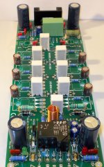
My LME49811 implementation.
http://i59.tinypic.com/de337p.jpg
http://i57.tinypic.com/rk4x94.jpg
http://i59.tinypic.com/2enu8gz.jpg
http://i60.tinypic.com/330e3rp.jpg
Regards,
Mircea.
http://i59.tinypic.com/de337p.jpg
http://i57.tinypic.com/rk4x94.jpg
http://i59.tinypic.com/2enu8gz.jpg
http://i60.tinypic.com/330e3rp.jpg
Regards,
Mircea.
Attachments

Last edited:
My LME49811 implementation.
http://i59.tinypic.com/de337p.jpg
http://i57.tinypic.com/rk4x94.jpg
http://i59.tinypic.com/2enu8gz.jpg
http://i60.tinypic.com/330e3rp.jpg
Regards,
Mircea.
Q3 Q4 C23 C24 circuit is it for current limiting?
Have you tried biasing it with mosfet at 1Amp?
I'm not really a fan of mosfet transistor type.
Class A is not for me. I become a little bit "green".
Regards,
Mircea.
Class A is not for me. I become a little bit "green".
Regards,
Mircea.
I'm not really a fan of mosfet transistor type.
Class A is not for me. I become a little bit "green".
In one of his articles, Nelson Pass discusses the paranoia of some purchasers of his amplifiers ... one supposedly could hear when it transitioned from Class A to Class AB.
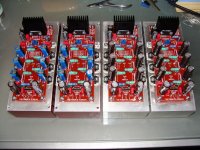
Here are some LME49830 modules from China using the Toshiba MOSFETs:
Attachments
Hallo, Mircea,
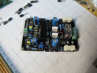
I quickly looked at the diagram in http://oi57.tinypic.com/rk4x94.jpg
and I think the potentiometer P1 should be put in parallel with C19, between the 2 resistors (R8, R9) on the basis of the drivers. Isn'it correct?
I quickly looked at the diagram in http://oi57.tinypic.com/rk4x94.jpg
and I think the potentiometer P1 should be put in parallel with C19, between the 2 resistors (R8, R9) on the basis of the drivers. Isn'it correct?

Hi Mircea,
Do you sell bare PCB's or would you like to share the Gerber files with me?
I would like to build it and test this amp.
Kind regards,
Peter
Do you sell bare PCB's or would you like to share the Gerber files with me?
I would like to build it and test this amp.
Kind regards,
Peter
Hi Mircea,
Do you sell bare PCB's or would you like to share the Gerber files with me?
I would like to build it and test this amp.
Kind regards,
Peter
I could send you two PCB's at production cost plus postage.
You can contact me by email.
Regards,
Mircea
Hi Mircea,
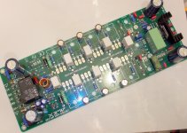
The board is very compact and and the components are neatly arrange. I have another question for you:
From the images available I did not see the component Rth NTC (thermistor) on the populated board (in the schematic is connected in parallel to potentioneter P1)
Is it an optional component?
Or it is foreseen for the thermal stablization of the output BJT bias current in case of use of BJTs without integrated diode for thermal track?
Best Regards,
Luigi
Hi Mircea,
Or it is foreseen for the thermal stablization of the output BJT bias current in case of use of BJTs without integrated diode for thermal track?
Best Regards,
Luigi
Hi Luigi,
Yes, it is for thermal stablization.
Unfortunately the diode inside ThermalTrak transistor is nothing else then ultrafast diode (MUR120).
However, in this configuration I have a very good thermal equilibrium.
Regards,
Mircea
Hi Mircea, Nice protection idea! have you tested the shortcircuit/overcurrent protection circuit?
Regards,
Peter
Regards,
Peter
"I quickly looked at the diagram in http://oi57.tinypic.com/rk4x94.jpg
and I think the potentiometer P1 should be put in parallel with C19, between the 2 resistors (R8, R9) on the basis of the drivers. Isn'it correct?"
"Your observation is right. In fact P1 is located between the ThermalTrak diodes."
So, the schematic is WRONG??
and I think the potentiometer P1 should be put in parallel with C19, between the 2 resistors (R8, R9) on the basis of the drivers. Isn'it correct?"
"Your observation is right. In fact P1 is located between the ThermalTrak diodes."
So, the schematic is WRONG??
if you redraw the sch with the diodes in between the bases of the drivers, you can see that the sch shows a series combination of a variable resistor in parallel to NTC resistor and then two diodes.
That combination is in parallel to C19
That combination is in parallel to C19
I sell a few Kits for who want to build a good amplifier.
Unfortunately, only in Europe.
Unfortunately, only in Europe.
An externally hosted image should be here but it was not working when we last tested it.
An externally hosted image should be here but it was not working when we last tested it.
I suggest that you secure the small heat sink mechanically to the board. Otherwise, vibration will cause the pins on the LME498xx to fail by metal fatigue.
Tom
Tom
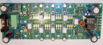
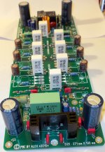
Just another amplifier LME 49810 driving 4 pairs OT 😀
Regards,Alex
Regards,Alex
Attachments

- Home
- Amplifiers
- Chip Amps
- Comparing LME49810, 49830 and 49811