Indeed I do.Measurement Numbers pls,................
I believe AndrewT has a LME49830 design using OPC wireamp, what is its noise measurement? ..............
I am listening to it now!
It measures 0.0mVac to 0.1mVac (it flickers between these readings spending slightly more time on the 0.0mVac reading), when the input is shorted or when the (very remote located) input vol pot is set to zero, even though it has never been fitted inside a screening Chassis.
My version is set up a bit differently from the OPC instructions. I am use SE AC and use 30k for upper feedback and Rin. I have 1k2 as lower feedback and Rseries. I have 330uF DC blocker on the 1k2 NFB and 2u2F DC blocker on the signal input.
I also have changed the grounding routes around R45 & R46. OPC PCB is wrongly configured here.
I have also piggy backed an RF filter cap on top of R46. And added an Output Zobel between the big decoupling caps. Lot's of changes before it ever reached a speaker.
Most of my power amplifiers never get as far as getting fitted inside a permanent chassis.
ps,
I have no pets, no kids, no wife with her duster, and it's obvious to my visitors that they should not "prod" my exposed gear.
Last edited:
Hi Guys,
Maybe out of topic but I want to ask about Vbe transistor type and polarity. I'm about to build an amp based on LME49811 and I have plenty of PNP driver transistors. So, I want to use PNP ones in place of NPN Vbe transistors those we see in schematics. Is it possible without any additional modifications? Is there any Vce rating requirement depending on rail voltages for this transistor?
Thanks.
Last edited:
PNP OK.
Bias voltage between the sink and source in a 811 is less than 5V. The transistor sees only this voltage.
Bias voltage between the sink and source in a 811 is less than 5V. The transistor sees only this voltage.
Hi all,
Is there anyone who tried lower gain settings than 26db with these chips?
I plan to build a bridged configuration with 12V peak-to-peak balanced source. Since my balanced signal level is relatively high, i think it would be a fair decision to use lower gain amp with such input signal especially in bridged configuration. Datasheet states we may occur instabilities with lower gains than 26db but I wonder anyone encountered any stability issue with lower gains as stated. I will use single pair of 150W Sanken darlingtons at each channel. Rails are +-35V dc.
I appreciate any comments on this.
Last edited:
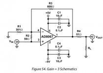
Here's an example of how to run a decompensated ( in this case a min-gain-of-8 AD8067) opamp at lower overall gain. The resistor to add is R2, here 50ohms. Its also permissible to put a cap in series with this resistor so that the DC offset and LF noise don't suffer.
Attachments
Here's an example of how to run a decompensated ( in this case a min-gain-of-8 AD8067) opamp at lower overall gain. The resistor to add is R2, here 50ohms. Its also permissible to put a cap in series with this resistor so that the DC offset and LF noise don't suffer.
Interesting approach..despite relying on amplification of noise instead of signal. What range of capacitor value is suffice in case of ~10K input impedance? According to AD datasheet, gain is 1+ [R3 / (R1||R2)], so.. does R1||R2 mean 1/R1+1/R2 or simply R1/R2?
Thanks.
Last edited:
R1||R2 means R1 in parallel with R2, so the reciprocal of your first suggestion.
For a cap in series with 50ohms, I'd initially try 1uF. I'd doubt you'd need such a low value R2 with the LMEs so the cap would decrease by the same amount as the R2 scales up.
For a cap in series with 50ohms, I'd initially try 1uF. I'd doubt you'd need such a low value R2 with the LMEs so the cap would decrease by the same amount as the R2 scales up.
The stability issue only rears it's ugly head at HF and generally this HF is well above the Audio Passband.
If you choose a resistor alone for R2 then the noise gain of the amplifier applies over the whole passband of the amplifier.
You can take advantage of the noise gain and only needing the stability of the noise gain at HF by using an R+C for R2.
Choose a capacitor that moves the majority of the noise gain above the audio passband.
If you are lucky (or can use a simulator) you will find that the audio passband becomes stable and the added noise of the high noise gain is only measurable above our HF limit.
There are many "stability" articles which describe this "noise gain" adjustment.
BTW, I am in the early part of my stability learning having only built one +20dB chipamp implementation. I can't hear any added noise and the amp plays very well. This method should work for +12dB chipamp implementations, but the added noise (due to larger cap value) may move down closer to the audio range.
If any one spots an error/s in my comments, please correct me.
Last edited:
Here is an another note about noise gain vs signal gain.
http://www.analog.com/library/analogDialogue/cd/vol46n4.pdf#page=3
They elaborated the technique in two different methods Method 1, Method 2. They notice the advantage of Method 1 because of lower noise comparing Method 2. It seems same advantage can be attained by adding a series capacitor (Cc) to R1 on Method 2.
Btw, the term of "decompensation" puts a question mark about external compensation capacitor of LM chips which is usually 30pf. Is this capacitor going to be superfluous in case of "decompensation"? or they are serve for entirely different things?
Edit: here is another document:
http://www.analog.com/library/analogDialogue/archives/31-2/appleng.html
Attachments

Last edited:
It's a lot of pages to read, so may I ask if someone can sum up what has been the result of this comparison?
I've seen some projects for the 49810 as a power amp's voltage amp stage, like this one:
http://4.bp.blogspot.com/-ODzkb_Cmq...I/6usdIHrpt4I/s1600/LME49810_HIGH_END_BIS.png
What do the others add to this?
I've seen some projects for the 49810 as a power amp's voltage amp stage, like this one:
http://4.bp.blogspot.com/-ODzkb_Cmq...I/6usdIHrpt4I/s1600/LME49810_HIGH_END_BIS.png
What do the others add to this?
Do they look like these? If so I have four ready to assemble into a stereo bridged pair (with step-down OPT) but haven't built the power supply yet. I'll report back when they're up and running.
I searched for a small LME pcb's like this but ended up with two stereo LM4702 pcb's. Seller sent me darlington/mosfet version mistakenly but no problem at all since I have enough amount of MN2488/MP1620 Sanken darlingtons. These chinese pcb's are very high quality.
Are these modules compatible with LME49811's? Where did you get them?
Edit: Ok, there are couple of listings at aliexpress. Probably this kit is quite new..
Last edited:
I've not investigated substituting the main IC so can't answer that at the moment. They came from this Taobao seller, he's in Chengdu - ·¢ÉÕ¼¶LME49810TB ÍƵ¥¶Ô¹Ü¹¦·Å Ó¡°å/Ì×¼þ/³ÉÆ·°å-ÌÔ±¦Íø
These are the kits I'm talking about:
1 PC LME49810 Top Audio Power Amplifier Board Mono 300W 1943 5200 | eBay
The output is handled by 1943+ 5200, so I'm not sure if they are legit or fakes.
1 PC LME49810 Top Audio Power Amplifier Board Mono 300W 1943 5200 | eBay
The output is handled by 1943+ 5200, so I'm not sure if they are legit or fakes.
Indeed I do.
I am listening to it now!
It measures 0.0mVac to 0.1mVac (it flickers between these readings spending slightly more time on the 0.0mVac reading), when the input is shorted or when the (very remote located) input vol pot is set to zero, even though it has never been fitted inside a screening Chassis.
My version is set up a bit differently from the OPC instructions. I am use SE AC and use 30k for upper feedback and Rin. I have 1k2 as lower feedback and Rseries. I have 330uF DC blocker on the 1k2 NFB and 2u2F DC blocker on the signal input.
I also have changed the grounding routes around R45 & R46. OPC PCB is wrongly configured here.
I have also piggy backed an RF filter cap on top of R46. And added an Output Zobel between the big decoupling caps. Lot's of changes before it ever reached a speaker.
Most of my power amplifiers never get as far as getting fitted inside a permanent chassis.
ps,
I have no pets, no kids, no wife with her duster, and it's obvious to my visitors that they should not "prod" my exposed gear.
Hi Andrew,
Can you explain why you think OPC 's the Wire grounding routes r45 (=0 ohm), r46 are wrongly configured? Can this possibly lead to the small 'hum whithout solution till so far' I'm having?
Greetz, Wimshurst
Hi, abraxalito
I am also very interested in the LME49810 Sanken boards. and i would like to see some test results.
Regards,
Peter
I am also very interested in the LME49810 Sanken boards. and i would like to see some test results.
Regards,
Peter
what is the actual difference between the lme49830 and lme49811. I liked the 811 than the 830 and 810. But I believe lm4702 and 811 and 830 have same architecture?
830 is just with added drivers to 811? I dont think so 811 and 4702 sounded very different but very similar.
Did anybody find this as 830 is not as good as 811? so reg 830 Is it just the drivers added to 811 ?
830 is just with added drivers to 811? I dont think so 811 and 4702 sounded very different but very similar.
Did anybody find this as 830 is not as good as 811? so reg 830 Is it just the drivers added to 811 ?
what is the actual difference between the lme49830 and lme49811. I liked the 811 than the 830 and 810. But I believe lm4702 and 811 and 830 have same architecture?
830 is just with added drivers to 811? I dont think so 811 and 4702 sounded very different but very similar.
Did anybody find this as 830 is not as good as 811? so reg 830 Is it just the drivers added to 811 ?
811 is the mono version of 4702 with slight layout changes. 830 is specifically designed to drive mosfet output stages. 810 is beefed up version of 811 but having a classAB driver stage (811 has class A stage) to deliver extra current and has some extra features like baker clamp . You can consider that 810 is designed for hall and concert audio reproduction systems and 811 for hifi systems. You can find comments of Audioman54, a former National employee, in forum regarding these chips.
Last edited:
- Home
- Amplifiers
- Chip Amps
- Comparing LME49810, 49830 and 49811