ZDR what is max voltage input rating? It's marked 50 on the what you shared. Can it do 53-56 MAX like Ti design?
Does it have full feature set of Ti original TPA3255?
50v is just a marking, it can go as much as tpa3255 can handle. This is only Stereo BTL, no other configs are planned.
Last edited:
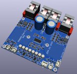
Don't tell me the speaker QD connectors are in between the power inductors?This amp definitely deserves and update, so here it is🙂
Two LM5017 for 5 and 12V, should run much colder. Optimized space for original TPA heatsink
1) I would strongly recommend making the board a bit longer and putting the connectors along the outside edge... and preferably Phoenix TDPT push-in (not screw) terminals instead 😉 Two of these, for example, if going with stereo BTL only: 1017503 Phoenix Contact | Mouser Canada
2) Also, would be really nice if the input connectors were compatible with MTA 100? Those are my favorite low-voltage connectors.
3) Mounting holes should be outboard of all connectors, in order to avoid cantilevered loads. Especially if using QD connectors. A stubborn connection could put quite a large amount of force on an unsupported free end of PCB.
4) Are the mounting holes grounded? If the board is able to accept single-ended inputs, it would be nicer to have the mounting holes isolated in order to allow free function of a ground loop breaker circuit.
5) Are there connections for multi-board synchronization to avoid beat interference? https://www.ti.com/lit/an/slaa787/slaa787.pdf
Last edited:
ZDR
I like it alot. I am not sure if a properly critical circuit load balanced amongst a 4 layered PCB would benefit the overall build but it seems in theory it would if implemented and integrated effectively. Should help circuit cooler and mitigate and regulate voltage quality.
FOR OPAMP if absolutely needed please use lowest impendence neutral reference design. I think the OPAMP technology may be out dated filters technology. With graphene nano technology this final signal magic may be improved.
Does this board do balanced XLR signal input?
Stereo BTL as a dedicated isolated design sounds perfect for its desired HIFI need.
Don't tell me the speaker QD connectors are in between the power inductors?
1) I would strongly recommend making the board a bit longer and putting the connectors along the outside edge... and preferably Phoenix TDPT push-in (not screw) terminals instead 😉 Two of these, for example, if going with stereo BTL only: 1017503 Phoenix Contact | Mouser Canada
2) Also, would be really nice if the input connectors were compatible with MTA 100? Those are my favorite low-voltage connectors.
3) Mounting holes should be outboard of all connectors, in order to avoid cantilevered loads. Especially if using QD connectors. A stubborn connection could put quite a large amount of force on an unsupported free end of PCB.
4) Are the mounting holes grounded? If the board is able to accept single-ended inputs, it would be nicer to have the mounting holes isolated in order to allow free function of a ground loop breaker circuit.
5) Are there connections for multi-board synchronization to avoid beat interference? https://www.ti.com/lit/an/slaa787/slaa787.pdf
1) Need to keep it 10cm max in all directions. Keeps cost down.
2) link? Connectors are JST 2.5mm pitch, many other with same pitch should fit in.
3) I would like to, but I need to keep board small, 10x10cm max. You can always use angled faston, so that pulling force is horizontal instead of vertical.
4) Mounting holes are isolated. Board can take SE and balanced inputs.
5) I will check it out.
In that case, it would be nice to have a through-hole adjacent to the QD to allow soldering of a 12-14 AWG stranded wire for direct connection to a panel output connector.1) Need to keep it 10cm max in all directions. Keeps cost down.
Example: https://www.mouser.ca/ProductDetail/TE-Connectivity-AMP/3-641238-3?qs=AplfTeSvkkDC8YY4zFO8bQ==2) link? Connectors are JST 2.5mm pitch, many other with same pitch should fit in.
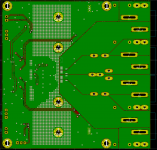
One small correction - edge holes are isolated, but heatsink holes are grounded.
6x Edge holes Isolated from earth as in leaky voltage run in circles with no escape by design?
2 heat sink holes designed to be grounded to path to the earth?
��
What does this mean? Like it would be better to have them act as antennae? (that's a joke)6x Edge holes Isolated from earth as in leaky voltage run in circles with no escape by design?
There is still (at least) one 0 V reference on the board even if the mounting holes are isolated, you know. For example, 0 VDC on the incoming DC power, and "common" (also 0 VDC) on the incoming signal(s).
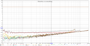
Some more measurements, with preamp in the loop, and cheap MLCCs in the signal path. I was expecting much more distortion from MLCCs in lower frequency range.
Attachments
Last edited:
I had played with Class-D TDA8920B chip.
Amplifier built like defined in datasheet. Sound ok but not top notch.
Made few improvements and these clearly made sound better:
1. good big output inductor(most noticeable improvement)
2. External quartz oscillator (most noticeable improvement)
3. Vaa (analog part TPA8920) supply been filtered and stabilised
4. Stabilized supply for Power part of TPA8920 (weakest impact on sound)
Maybe TPA3255 could be improved in same way.
I wondering it will be good to use separate regulators for Vdd and GVdd, try external clock.
Maybe use capacitance multiplier for PVdd. "Volt+" did this for TPA3116 and it measures perfect:
Allo Volt+ D Amplifier Review | Audio Science Review (ASR) Forum
The article quoted shows 0.006 THD at 1KHz for Volt+, I measured 0.0016. As I said, does not get much better than this. I am not touching it any more🙂 I am not sure if I should replace LT3012 at all with buck regulators, I could only mess up something with unwanted noise down the rails. Separate regulators for VDD voltages, why do you think that would make any difference? They are going into the same IC after all. I might cascade two LT3012 to spread the dissipation around and clean up the voltage even more, but some people have expressed concerns about the cost of LT3012.
When I put everything together, I might send it to audiosciencereview🙂
When I put everything together, I might send it to audiosciencereview🙂
I would do in this way:
no buck converters at all.
From PVDD to Zener + transistor (let be MJE15030 or D44H11) regulator to make some 20V. Then follow low noise regulators for 12V.
I'm suspecting that GVDD put some noise back and VDD could have that at input. Just for assurance would better to have two regulators.
I red DIY thread about TPA3255 and looks like DrMordor implemented in this way.
I have auxiliary out in PSU, 20V and 3 separated LDO, GVDD, AVDD, opamp'sI red DIY thread about TPA3255 and looks like DrMordor implemented in this way.
The article quoted shows 0.006 THD at 1KHz for Volt+, I measured 0.0016. As I said, does not get much better than this. I am not touching it any more🙂 I am not sure if I should replace LT3012 at all with buck regulators, I could only mess up something with unwanted noise down the rails. Separate regulators for VDD voltages, why do you think that would make any difference? They are going into the same IC after all. I might cascade two LT3012 to spread the dissipation around and clean up the voltage even more, but some people have expressed concerns about the cost of LT3012.
When I put everything together, I might send it to audiosciencereview🙂
Hi Zdr,
Very nice amp! Congrats. Can you give more details for your distortion measurement? The TI PFFB app note quotes one of the reference conditions of 10Wrms BTL config with a 48v supply with 0.0021% THD. So if your measurement is at 10wrms and you get 0.0016% beats that. It comes down to layout and quality of components. On my amp with PFFB, I managed to get 0.0011% THD for 10wrms.
I think the big SER29X Coilcraft falt copper wire inductors and the layout play a significant role.
Last edited:
Thanks! The measurement was done at 10W, 4.5ohm, 20V, Lenovo laptop PS. Passive components are cheapest AliExpress ones I found in the drawer, the coils are coilcraft knockoffs and there are even MLCCs at the amp inputs 🙂
PCB is also standard with 1oz copper.
PCB is also standard with 1oz copper.
What does this mean? Like it would be better to have them act as antennae? (that's a joke)
There is still (at least) one 0 V reference on the board even if the mounting holes are isolated, you know. For example, 0 VDC on the incoming DC power, and "common" (also 0 VDC) on the incoming signal(s).
I was just asking for clarity on how the 6 edge holes are isolated and how the 2 heat sink holes are grounded.
It wasn't clear to me. I'm not sure what the isolation holes and grounding holes do as designed.
Thanks! The measurement was done at 10W, 4.5ohm, 20V, Lenovo laptop PS. Passive components are cheapest AliExpress ones I found in the drawer, the coils are coilcraft knockoffs and there are even MLCCs at the amp inputs 🙂
PCB is also standard with 1oz copper.
I see no harm in going with at least a 4 layer 2 ounce copper PCB as long as you use the layers effectively to further balance voltage loads of circuit e.g. you could split up left and right channel distribution to help isolate electrical noise and help dissipate heat. Also I think lower impedance coils might possibly improve performance. I'm interested in layered graphene as first contact between copper PCB layers to help with thermal cooling of circuit voltage in copper PCB.
I like the layout of your board so far.
I've never built and audio amplifier before and I appreciate your time and testing to provide good audio amplifier IC module.
Thanks! The measurement was done at 10W, 4.5ohm, 20V, Lenovo laptop PS. Passive components are cheapest AliExpress ones I found in the drawer, the coils are coilcraft knockoffs and there are even MLCCs at the amp inputs 🙂
PCB is also standard with 1oz copper.
That’s pretty good for cheap AliExpress parts. I am using 2oz copper, all name brand metal thin film resistors (Vishay etc), no MLCCs in signal path (Elna Silmic II 10uF), and real CoilCraft SER290x series inductors. I think the inductors make a big difference. So the quality parts do help to bring down the distortion vs no name parts.
- Home
- Amplifiers
- Class D
- Compact TPA3255 design with PFFB and single PS