I don't use ceramic capacitors for clock bypass at all. That includes for clock module adapter boards made by Iancanada, Twisted Pear, and or others.
However, if you want to try Panasonic SMD film caps on the adapter board, I would suggest to first give the clock and reclocker board some time as is with the MU cap. Then after letting the clock run for a few days just with the MU bypass cap, then maybe try adding the Panasonic film cap to see if it gives any improvement in sound. I would suggest to let the dac run overnight with the added cap so the cap has time to settle in, then see what you think.
However, if you want to try Panasonic SMD film caps on the adapter board, I would suggest to first give the clock and reclocker board some time as is with the MU cap. Then after letting the clock run for a few days just with the MU bypass cap, then maybe try adding the Panasonic film cap to see if it gives any improvement in sound. I would suggest to let the dac run overnight with the added cap so the cap has time to settle in, then see what you think.
Last edited:
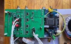
Hi, I am not sure what headers must order to connect the reclock v15 to my PCM2DSD module. As stated in the PDF doc, shoud be placed underneath, allright but my interface "PCM2DSD Amanero" is already plugged underneath to the toslink receiver module. Please see photo atch.
Another question, please, I see another 2x10 header in the BOM, to connect V15 to "PCM2DSD DSC". Same problem, I have this row occupied also by a female header plugged to the Firdac DAC.
Jordi
Another question, please, I see another 2x10 header in the BOM, to connect V15 to "PCM2DSD DSC". Same problem, I have this row occupied also by a female header plugged to the Firdac DAC.

Jordi
Connections from Cestrian's Clock and Reclocker board to Marcel's RTZ dac are by u.fl connectors. In the pic you posted you are not using Marcel's input u.fl connectors. Please take a look at the example pics earlier in Cestrian's thread to see where each board is located.
Some pics showing the u.fl cables at: https://www.diyaudio.com/community/...2soverusb-pcm2dsd-rtz-dac.423401/post-7998454
And at: https://www.diyaudio.com/community/...2soverusb-pcm2dsd-rtz-dac.423401/post-8002796
Some pics showing the u.fl cables at: https://www.diyaudio.com/community/...2soverusb-pcm2dsd-rtz-dac.423401/post-7998454
And at: https://www.diyaudio.com/community/...2soverusb-pcm2dsd-rtz-dac.423401/post-8002796
Good, I see 3 U-fl connectors as v15 output, so why the 2nd 2x10 pin header ( PCM2DSD DSC ) in the BOM? That's useful to secure mechanical?
I miss picture example using Dsd2pcm.
Still not sure how to plug my Toslink receiver to the PCM2DSD and to the V15 input all togheter in the same I2S row interface.
I miss picture example using Dsd2pcm.
Still not sure how to plug my Toslink receiver to the PCM2DSD and to the V15 input all togheter in the same I2S row interface.
PCM2DSD is hanging under the bottom of Cestrian's board. So, its like I2SoverUSB is on top, Cestrian's board is in middle, and PCM2DSD is down below where you can't really see it. But you can see where there are holes in Cestrian's board to add pin headers sockets on the bottom in order to be able to plug in PCM2DSD down there.
Regarding your TOSLINIK receiver, that's a bit complicated. You have two problems. First problem is that you would need to remove the I2SoverUSB board and attach your TOSLINK receiver board to Cestrian's board there (somehow or other). The second problem is you need a copy of one of the MCLK signals from Cestrian's board to replace the clocks on your TOSLINK board. Actually, there is a third problem too: You need to take the signal that switches between clocks on the TOSLINK receiver board, and use that signal to tell Cestrian's board when to switch his clocks. That will make the TOSLINK receiver board I2S output synchronous with Cestrian's clocks.
Once all the above is done, then you need to make sure the I2S signals going into Cestrian's reclocker circuitry are arriving at the correct time. You may need a fast (100MHz) scope to see if there is any problem with timing there. If so, then we may have to take some measurements to figure out how to fix the timing a little.
Last edited:
So I must plug both 2x10 pin headers, thanks confirm.
But I don't know how to solve connect three I2s at same place.
The PCM2DSD has an input I2S row (version 1 without U-fl).
What mouser part can allow me plug there two more I2S interfaces, one at each side?
But I don't know how to solve connect three I2s at same place.
The PCM2DSD has an input I2S row (version 1 without U-fl).
What mouser part can allow me plug there two more I2S interfaces, one at each side?
You do not connect three I2S sets of signals at the same place. I2SoverUSB has two sets of pin headers. PCM2DSD has two sets of pin headers. There are normally no shared pin headers with I2S signals.
Now, if you want to use your TOSLINK board, then you have to remove I2SoverUSB, and connect the TOSLINK board instead. It might be easier to if you made an adapter board to convert your TOSLINK board to I2SoverUSB pinout. Also, in theory you could use an Amanero USB board with your TOSLINK board. While that could be done instead of using I2SoverUSB, its probably not a good idea.
If you want to be able to switch quickly between USB and TOSLINK without swapping out boards, then that's another problem. Cestrian's board wasn't designed to work with your TOSLINK board, so its something you would have to custom adapt if you want to use Cestrian's board.
As can be seen below, there are two sets of two pin headers on Cestrian's board:

The purple box shows where PCM2DSD plugs into the bottom of Cestrian's board. The red box shows where I2SoverUSB plugs into the top of Cestrian's board.
If you want to connect up your TOSLINK board instead of using I2SoverUSB, the you would patch your TOSLINK board into the pin headers normally used by I2SoverUSB (which are on top).
Now makes sense, the Toslink receiver replaces I2SoverUSB!
Thanks patience Mark, going to complete the Mouser order!!😊
Thanks patience Mark, going to complete the Mouser order!!😊
My receiver board do not have troaught holes to keep placing the output I2S header underneath.
But not bother that much because are neither pin compatible.
How many pins I need to wire to the V15 reclock?
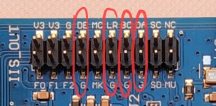
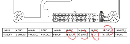
Please see atch., my guess is those four pairs circled in red marker (three I2S pairs +DSD pair)
Anything else is mandatory to wire, Mute maybe?
But not bother that much because are neither pin compatible.
How many pins I need to wire to the V15 reclock?
Please see atch., my guess is those four pairs circled in red marker (three I2S pairs +DSD pair)
Anything else is mandatory to wire, Mute maybe?


Last edited:
It depends. You will necessarily need the three I2S bus signals and their grounds. Also:
1. Will you be using PCM2DSD? If so, then you will need a 22/24MHz MCLK signal for it that is in phase with the I2S signals you are sending.
2. You will need to hack the TOSLINK board to accept an external MCLK signal as the reference clock for the ASRC, and you will need to determine what frequency clock(s) it will need.
3. You will need to hack the TOSLINK board to export a clock select bit for the needed clock family (or else program the ASRC chip to work with only one reference clock frequency).
What are the frequencies of the two clocks on your TOSLINK board? It should be written on them, but you might need a magnifier to see it. They should either be 22/24MHz or else 45/49MHz. The type of board you have was made in different models having one set of clock frequencies or the other.
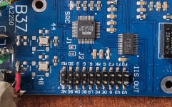
The pic above is probably almost enough to explain what needs to be done, but the board is pretty dirty. It would be more clear if you could clean off the board with some alcohol or flux remover then take another pic of the same area, or maybe a little wider view. We need to see the clocks, the AK4137 chip, and the pin header a little better. Most of what we will be talking about is almost fully shown in the existing pic, but maybe not quite. Also, we will need to be able to see the traces in clear focus.
Here is some info you may need to know:

IIRC, the purple arrow shows where a trace on the bottom sends the selected clock output to the reference input terminal on AK4137.
The red arrow shows where a trace on the bottom connects to the MK (master clock) output on the pin header.
J1 and J2 select whether to send the crystal clocks, or else to send the MCLK output from AK4137 to the MK pin header terminal.
To bring in an external clock signal, maybe the easiest way is to remove the two resistors shown in green boxes, then bypass the clock doubler on Cestrian's board so that you can bring in 22/24MHz clocks (and the ground) from Cestrian's board to this board using one of the 33R resistor pads connected to the purple arrow reference clock trace.
To get a signal from this board to switch clocks on Cestrian's board, you can take a signal from the pad in the yellow box. That signal should be high when the 22MHz clock is selected. The inverse clock select signal could be taken instead from the corresponding pad for the existing 24MHz clock.
Also, you should probably remove power to the clocks on this board, when you bring in a clock signal from Cestrian's board.
The MK pin on the head should then go the MCLK pin one PCM2DSD. Which clock source you should select (solder jumper J1 or J2) is whichever one makes PCM2DSD work properly. I don't recall offhand exactly how the MCLK output signal from AK4137 is derived. Maybe AK4137 MCLK output will be in better sync with AK4137 I2S outputs than the reference clock signal will be. Have to check the datasheet on that.
Last edited:
Thanks no need to say, I see the overall picture with some variables but not going to bother, as yet still completing the BOM order.
I understand better to add some more U-fl cables for just in case.
If it is a chance the AK4137 doesn't want be in sync, then I would like to play and hear that in first. In such a case, will it run everything flawless?
Concerning the Cestrian's reclock, from where I should pick the clock signal, how to bypass the clock doubler...
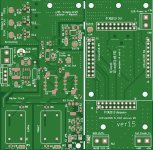

To bypass the clock multiplier:

On Cestrian's board, solder pads 1&2 together on solder jumper JP1, as shown in the blue box above.
The 22/24MHz MCLK signal will then appear on u.fl connector J16 (and on J17). It will also appear on Pin-3 of the I2SoverUSB pin header (as shown in the I2SoverUSB datasheet, and in Cestrian's schematic).
There is a pretty good chance it will just work if you hook it up in the way I suggested. If not, then it might be necessary to look at some signals with an oscilloscope to see what we need to do.
- Home
- Source & Line
- Digital Line Level
- Clock & Re-clocker and interface board for JLSounds I2SoverUSB -> PCM2DSD -> RTZ DAC


