push-pull drivers
Hi Damir,
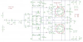
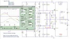
Here it is. Red encircled are the PP-drivers and left to the 1X buffer the 2nd order LP filter. (btw, this amp is not complete).
With this synthetic 1x buffer you can push the amp to much higher slew rates. But, as said already, not without dangerous cross-conduction.
If you put the LP-filter in front of the pre-amp, it has to modified (of course).
Cheers,
E.
edit: The crux is the crosswise connection of R23 & R24.
Hi Edmond,
Could you show the circuit?
Damir
Hi Damir,
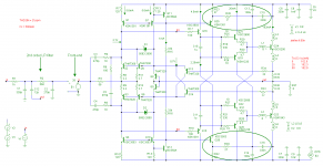
Here it is. Red encircled are the PP-drivers and left to the 1X buffer the 2nd order LP filter. (btw, this amp is not complete).
With this synthetic 1x buffer you can push the amp to much higher slew rates. But, as said already, not without dangerous cross-conduction.
If you put the LP-filter in front of the pre-amp, it has to modified (of course).
Cheers,
E.
edit: The crux is the crosswise connection of R23 & R24.
Attachments
Last edited:
Hi Damir,
Here it is. Red encircled are the PP-drivers and left to the 1X buffer the 2nd order LP filter. (btw, this amp is not complete).
With this synthetic 1x buffer you can push the amp to much higher slew rates. But, as said already, not without dangerous cross-conduction.
If you put the LP-filter in front of the pre-amp, it has to modified (of course).
Cheers,
E.
edit: The crux is the crosswise connection of R23 & R24.
Hi Edmond,
It looks great, I will try it in my simulation soon.
Damir
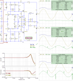
Yes. It (auto biased) work with 3906-3904.
Good slew rate but 9540 is just big gate caps charged with only 34mA.
Input is light error corrected and FFT around 0.004%THD all freq to 20k.
Good slew rate but 9540 is just big gate caps charged with only 34mA.
Input is light error corrected and FFT around 0.004%THD all freq to 20k.
Attachments

Last edited:
Hi Damir,
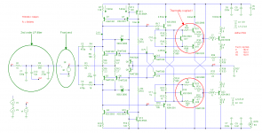
In case you incorporated also a front-end (with a gain of 28x), here's the modified LP-filter.
Hope it works; good luck. FYI, it's a Sallen-Key filter.
Cheers,
E.
Hi Edmond,
Thermal fluctuation of the PP drivers will not influence thermal stabillity of the output transistors, I suppose?
Damir
Yes. It (auto biased) work with 3906-3904.
Good slew rate but 9540 is just big gate caps charged with only 34mA.
Input is light error corrected and FFT around 0.004%THD all freq to 20k.
Hi ontoaba,
Amazing that even a minimalistic implementation, like yours, does work.
Nevertheless, I urge you to insert push-pull drivers between the bias circuit and MOSFETs (because of high Cgd and Cgs).
Cheers,
E.
May be I am doing wrong, I need pre EC to correct voltage gap and it work with 4148 too.😕
Hi, Damir.
Output stage is never turned off, up to 20kHz (my pict), looks like output transistor bias determined by AB circuit not heatsink temp.
Hi ontoaba,
Nice implementation. I know how AB works from simulation Edmond AB2 and Kendall Class i.
Damir
Hi Edmond,
Thermal fluctuation of the PP drivers will not influence thermal stabillity of the output transistors, I suppose?
Damir
Hi Damir,
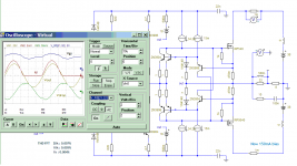
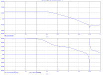
That's correct. Iq of the OPS is firmly stabilized by the high DC gain of the common mode NFB loop (51dB), see 1st pic.
The 2nd pic shows the differential loop gain and phase. This NFB loop determines to what extent the distortion is reduced.
The wild phase fluctuation at 100MHz worries me a bit, but I don't know (yet) how to tame it. Also, I don't know if it is really harmful.
Cheers,
E.
Attachments

Ahh... found it. I wrongly connecting colectors of first stage feedback bjts, silly😀. Now it is done, no crossover distortion anymore. Yes it is more simple and doesn't need that what any longer. Easier to design with that resistors available with wide values.
Attachments
Alternatives
Hi Mir,
Nothing wrong with your English. I think I do understand you quite well.
Regarding you suggestion -resistors parallel or in series with Q3 and Q5- I don't think it will have much effect. The points is, which is not so obvious at first sight, that the voltage across Q3 and Q5 is already held constant by the action of a large amount of feedback. Differential fluctuation of Vbe(Q3) and Vbe(Q5) is very small: only a few mV. If I keep the Vbe's really constant (by means of 1F caps across Q3 & Q5), THD20k is just the same.
I also replaced Q3 and Q4 by appropriate resistors. However, to no avail. Distortion gets even worse.
Cheers,
E.
Hi Edmond
Your post #18-19 is highly informative (I think not only for me), especially about the huge reduction of error due to the crossconnection on Fig.4.
Now let’s return to the “offsetless” Fig.3, which also is the simplest cirquit. Assuming Out grounded, consider e.g. the upper half of the cirquit an amplifier with emitter of Q1 as noninverting input, base of Q1 as inverting input, and Q5Q3 as a nonlinear divider in a local NFB loop. Resulting nonlinearity of this amplifier is presented by a red curve in Fig.7 and is responsible for all errors (black curve).
So almost the only thing determining errors is the nonlinearity of the divider between nodes S1 and A, and the simplest way to change (correct) the pattern of this nonlinearity is to place resistors in parallel or in series with Q5 and/or Q3 (with necessary variations of I3, of course). May be, this can give even better results than the crossconnection, or improve effect of the crossconnection itself.
You have already simmed similar changes, but mostly around Q1 (e.g. in #429 of HEEEELLLPPP and earlier). Why not to do some more experiments?
Cheers
Mir
Hi Edmond
Once again my poor English leads to possible misunderstanding. It is because the posts to this thread are the first attempts of English language conversation on technical issues for all my life. I’ll make another try some days later.
Cheers Mir
Hi Mir,
Nothing wrong with your English. I think I do understand you quite well.
Regarding you suggestion -resistors parallel or in series with Q3 and Q5- I don't think it will have much effect. The points is, which is not so obvious at first sight, that the voltage across Q3 and Q5 is already held constant by the action of a large amount of feedback. Differential fluctuation of Vbe(Q3) and Vbe(Q5) is very small: only a few mV. If I keep the Vbe's really constant (by means of 1F caps across Q3 & Q5), THD20k is just the same.
I also replaced Q3 and Q4 by appropriate resistors. However, to no avail. Distortion gets even worse.
Cheers,
E.
I am also reading miralin's posts, and don't know exactly, but he says something about improvement in linearity or better crossconnection configuration. I still try to read it again.
Anyway, this just for fun.
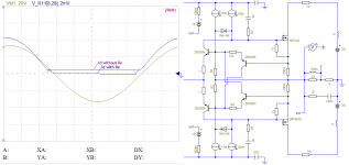
5ppm 1khz with only 15mA biased output stage. Ofcourse it using pre EC circuitry that could give 3ppm all freq up to 20k if using 200mA bias.
Anyway, this just for fun.
5ppm 1khz with only 15mA biased output stage. Ofcourse it using pre EC circuitry that could give 3ppm all freq up to 20k if using 200mA bias.
Attachments
I am also reading miralin's posts, and don't know exactly, but he says something about improvement in linearity or better crossconnection configuration. I still try to read it again.
Hi ontoaba,
As far as I understand, he worries about the nonlinearity of Q3 and Q5. In the meantime I've replaced them with several distotionless components, but distortion stays just the same. So I concluded that the contribution to distortion from Q3 ad Q5 is negligible or at least below 0.1ppm.
Anyway, this just for fun.
5ppm 1khz with only 15mA biased output stage. Ofcourse it using pre EC circuitry that could give 3ppm all freq up to 20k if using 200mA bias.
>just for fun 😕
I don't think so. You are are killing my baby in the most cruel way.

Merry Christmas!
E.
Last edited:
This with the use of diodes for making the output nonswitching is very much in line with Ken Peter's explorations....seems rather interesting...
Overkill and plain wrong. No need for Schottky's to make it non-switching.
Read his paper and my website first.
In any respect, that 'funny' circuit wrong, totally!
Read his paper and my website first.
In any respect, that 'funny' circuit wrong, totally!
Ok,
Thanks, so he says that non linearity caused by Q3 and or Q5, I could try to replace that 4148 in my circuit with just resistor and make Re of input transistor much higher. I'll try with that, but I see that THD20k is not caused by non linearity but something or part of circuit timing errors. It need to be corrected.
Hi, don't worry.
They are just an accessories for your baby, it won't kill, I think. Ok, my apologize and schottky removed🙂
With 1N4148s you need diode - transistor matching, a mission impossible.
I've tried hundreds of alternatives and believe me, the original AB2 circuit on post 41 is the best (as far as the bias circuit is concerned. The BJT output stage is another story. I prefer MOSFETs)
I've tried hundreds of alternatives and believe me, the original AB2 circuit on post 41 is the best (as far as the bias circuit is concerned. The BJT output stage is another story. I prefer MOSFETs)
The BJT output stage is another story. I prefer MOSFETs)
Please show mosfet version.
Which of the transistors should be thermal coupled?
- Status
- Not open for further replies.
- Home
- Amplifiers
- Solid State
- Class i and siblings