Dead zone is reduced with the D1 + R5 bias, Vbb bias is now 0.8V instead of 0V and the opamp has less work with distortion reduction.
Concept only. Use transistors with very low turn on volts (Germanium 😉) and scale the feedforward resistor such that the opamp output current is not exceeded at maximum output current.
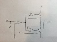
Parallel opamp could work well here. Voltage gain set to unity to maximise feedback factor for correction. 20kHz shown.
Lets try Lateral FET's...


Parallel opamp could work well here. Voltage gain set to unity to maximise feedback factor for correction. 20kHz shown.
Lets try Lateral FET's...
The 21st Century, the 3rd Millennium. Jenghis? Are you serious, man🙂? Nothing personal really, but....? This question reminds me of an exciting story about ''my transistors keep burning''. Anyway, it was a long time ago - 1981-2 y, around this time. If you want start here - the link below:
https://ldsound.info/usilitel-stonecold-200-vt4-om/
G. Schmidt, ''Current dumping amplifier'', ''Stonecold'' etc. Just some example. I think it's a good starting point
https://ldsound.info/usilitel-stonecold-200-vt4-om/
G. Schmidt, ''Current dumping amplifier'', ''Stonecold'' etc. Just some example. I think it's a good starting point
This of course MUST help. How about a usual gain of 26 - 28 dB?Voltage gain set to unity

Jenghis is prepared to use two op-amps, so using one for the voltage amplification and the other for the output buffer is a valid option.
The 21st Century, the 3rd Millennium. Jenghis? Are you serious, man🙂? Nothing personal really, but....? This question reminds me of an exciting story about ''my transistors keep burning''. Anyway, it was a long time ago - 1981-2 y, around this time. If you want start here - the link below:
https://ldsound.info/usilitel-stonecold-200-vt4-om/
G. Schmidt, ''Current dumping amplifier'', ''Stonecold'' etc. Just some example. I think it's a good starting point
Hahaha yes I have much to learn. I am drawn to these dead simple circuits, even though they typically need improvement.
I will look into this current dumping scheme further.
Less good as expected.This of course MUST help. How about a usual gain of 26 - 28 dB?
I have redrawn the schematic based on suggestions made by Marcel and Mooly. It might be a bit difficult to read, but basically I have used the lower value feed forward and feedback resistors as well as adding a a unity gain op-amp section slaved to the first one. Should the second op-amp output be connected to only its own 68ohm feed forward resistor, and not to the bases of the transistors?
It's far from elegant, but I want to see this circuit work properly with minimal changes.

If this circuit doesn't get close to a "hi-fi" sound, then I will look at adding diodes for bias or a current dumping topology.
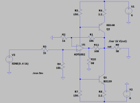
I'd also like to try Mooly's version with MOSFETs, but I'll have to see if I have any suitable power MOSFETs in my parts bin.
It's far from elegant, but I want to see this circuit work properly with minimal changes.
If this circuit doesn't get close to a "hi-fi" sound, then I will look at adding diodes for bias or a current dumping topology.
I'd also like to try Mooly's version with MOSFETs, but I'll have to see if I have any suitable power MOSFETs in my parts bin.
Yes, it is like rob Peter to pay Paul, but of course you have full right to do what you want to do. Blind alleys are a necessary part of DIY 😉.It's far from elegant, but I want to see this circuit work properly with minimal changes.
They are lateral power FET's rather than the more common MOSFET. In fact the circuit doesn't seem at all happy with MOSFET's in the simulation and just oscillates even when gate stopper resistors are used.I'd also like to try Mooly's version with MOSFETs, but I'll have to see if I have any suitable power MOSFETs in my parts bin.
You might get away with this. May or may not be strictly class B, depending on the offset voltages of the op amps. But the offsets are far lower than a Vbe, and it will needs some emitter resistance to absorb the effects of th offset, which could result in a small bias current. It does require each output to be slaved to its own op amp, requiring three. Could get pretty decent if using R2R op amps. Kind of got the idea from the 1EF thread where they use power op amps to directly drive 0281/0302. In that thread, there was a bias stack inserted ahead of the buffers and run in AB.
Attachments
I wonder what effect the base-emitter capacitances or a deliberately placed capacitor of about 1 nF to 2.2 nF between bases and emitters could have. It also acts as a feedforward path when the transistors are off, but hardly conducts any current when one of them is on (as variations in the base-emitter voltage are then relatively small), so almost all the op-amp's output current is then available as base current.
Suppose you have an op-amp with 20 V/us slew rate and 40 mA maximum output current (right order of magnitude for an LM4562). A 2 nF capacitance then suffices to conduct all its output current when it slews. Those power transistors probably have hundreds of picofarads of base-emitter capacitance at 0 V, and it increases when the base-emitter junction is slightly forward biased, like PMA does.
Suppose you have an op-amp with 20 V/us slew rate and 40 mA maximum output current (right order of magnitude for an LM4562). A 2 nF capacitance then suffices to conduct all its output current when it slews. Those power transistors probably have hundreds of picofarads of base-emitter capacitance at 0 V, and it increases when the base-emitter junction is slightly forward biased, like PMA does.
Actually it's class C in that each device conducts less than 180°. TheThat s exactly that, a true class B amplifier, meaning that there s no output stage current biasing, as such it will produce a lot of
crossover distorsion even if the op amp is of good perfs, you would be better building a similar amp using a pair of TDA2030 or 2040, you wouldnt even need additional transistors.
feedback is trying to fix that 'hole'. That's why it sounds bad.
G²
You should look at "Current Dumping" such as Quad 405, which has 0 bias at the last stage with very low distortion.
I wonder what effect the base-emitter capacitances or a deliberately placed capacitor of about 1 nF to 2.2 nF between bases and emitters could have. It also acts as a feedforward path when the transistors are off, but hardly conducts any current when one of them is on (as variations in the base-emitter voltage are then relatively small), so almost all the op-amp's output current is then available as base current.
Suppose you have an op-amp with 20 V/us slew rate and 40 mA maximum output current (right order of magnitude for an LM4562). A 2 nF capacitance then suffices to conduct all its output current when it slews. Those power transistors probably have hundreds of picofarads of base-emitter capacitance at 0 V, and it increases when the base-emitter junction is slightly forward biased, like PMA does.
That is, maybe PMA doesn't see an improvement with 150 ohm because there is already more current flowing through the base-emitter capacitances than through that resistor when the circuit is going through the crossover region. I don't know, it's just a hypothesis.
We old timers have played with these things a lot. Using an op-amp IPS has the following issues:
1. Limited supply voltage. High voltage op-amp exist but the point of this is cheap and common parts.
2. The output saturation voltage of common op-amps is already limited, and adding an EF makes it worse, although not so much if the bias stack is driven in the middle and bootstrapped.
3. Common op-amps are compensated for unity gain by themselves with no extra stages added, so stability can be a problem.
I have a b-zillion simulations I could post, but something missing in this thread so far is a supply pin driven common emitter output. The biggest problem with it is that he op-amp supply current has to be matched with the OP base resistors. I should also mention that one stage between an op-amp and an 8 Ohm load is not really enough.
Attachments
Well, very much depends on how you define the classes - if you define class B as a 180 degree conduction angle, this is close to the lowest distortion point... Some people call that AB though. The original circuit in this thread has less than 180 degree conduction angle, which arguably is class C.Class B is unsuitable for audio. Class AB requires only a few more components.
Ed
So it pays to be precise about the biasing, not just give a letter. For example standard emitter-follower power amplifier outputs are biased to around 50mA per device. CFP outputs to 10mA or so. Both are empirically determined to be lowest distortion points for those systems, and close to 180 degree conduction angle. Biasing EF to 10mA and CFP to 50mA give poorer performance, so you can't really assign classes to those bias points without explaining the nature of the output devices.
We old timers have played with these things a lot. Using an op-amp IPS has the following issues:
1. Limited supply voltage. High voltage op-amp exist but the point of this is cheap and common parts.
2. The output saturation voltage of common op-amps is already limited, and adding an EF makes it worse, although not so much if the bias stack is driven in the middle and bootstrapped.
3. Common op-amps are compensated for unity gain by themselves with no extra stages added, so stability can be a problem.
I have a b-zillion simulations I could post, but something missing in this thread so far is a supply pin driven common emitter output. The biggest problem with it is that he op-amp supply current has to be matched with the OP base resistors. I should also mention that one stage between an op-amp and an 8 Ohm load is not really enough.
Those are good points for sure. It looks like this circuit is good for playing around with on the breadboard, but not worth any serious application.
Yes, now you got it correct. It is a toy, toy circuit, not something to be used as a home amplifier. Of course even toys have some sense, but, as it is getting complex, the only value, simplicity, is lost and you do not get an advantage of much better parameters. The only challenge, from my point of view, is to keep it simple, but usable, with acceptable distortion.
- Home
- Amplifiers
- Solid State
- Class B Circuit Opinions...