A lot of people, like you, didn't understanding it properly until that paper was published from the University of Waterloo. I have a copy but was unable to upload it yesterday.
AES Journal Forum >> Feedforward Error Correction in Power Amplifiers
I cannot access that paper.
Are you able to explain why you think I don’t understand how the Quad 405 works. In a thread a while back I simulated it. It may be you are using a different definition of feed forward.
Member
Joined 2009
Paid Member
I tried to upload it without luck, but I’ll email it to you later.
The Quad also used negative feedback. From what I can tell, this feedforward implementation can’t be realized without including negative feedback (needed to accurately fix the gain and control impedances at the bridge where the signal and it’s correction are combined). However, I believe it could be implemented without negative feedback in a current mode output.
The Quad also used negative feedback. From what I can tell, this feedforward implementation can’t be realized without including negative feedback (needed to accurately fix the gain and control impedances at the bridge where the signal and it’s correction are combined). However, I believe it could be implemented without negative feedback in a current mode output.
There is a 0.6V dead zone, otherwise it wouldn't be a class C part, and in that dead zone the class A part provides all the current. The class C part supplies basically all the current when it is on, but not when it isn't.I do not see the class A stage as supplying the current in the dead zone of the class C stage. To me, the class C stage is supplying the major part of current when the class A stage can't provide it enough. Then both currents sum into the load. Maybe we can say that the class A commands and the class C obeys. All this is under the control of the balanced bridge which role is to obtain a constant output impedance, be the class C stage delivering current or not.
That’s not what feed-forward is, tho. This is like a current bootstrap on a LM317 regulator except the regulator outputs a current. The output voltage is controlled by feed-back.I tried to upload it without luck, but I’ll email it to you later.
The Quad also used negative feedback. From what I can tell, this feedforward implementation can’t be realized without including negative feedback (needed to accurately fix the gain and control impedances at the bridge where the signal and it’s correction are combined). However, I believe it could be implemented without negative feedback in a current mode output.
I’ve read that paper before and commented on it. I found it a turgid read. They really could have explained the thing more succinctly. Publicists.
And this presents a limitation on its load. Too low and the class A will saturate before the bootstrap transistors turn on.There is a 0.6V dead zone, otherwise it wouldn't be a class C part, and in that dead zone the class A part provides all the current. The class C part supplies basically all the current when it is on, but not when it isn't.
The class A still provides voltage and current to bias the class C transistors.There is a 0.6V dead zone, otherwise it wouldn't be a class C part, and in that dead zone the class A part provides all the current. The class C part supplies basically all the current when it is on, but not when it isn't.
The class C bootstraps the class A output.
The role of the bridge is fundamental : it assures a constant output impedance when only class A is on as well when a transistor of the class C is conducting.
Last edited:
is the class G of Hitachi not AB+C ?
Class-G Power Amplifiers
Classes d'amplification
I'm going to take an aspirin, my head hurts...
Class-G Power Amplifiers
Classes d'amplification
I'm going to take an aspirin, my head hurts...
The class A still provides voltage and current to bias the class C transistors.
The class C bootstraps the class A output.
The role of the bridge is fundamental : it assures a constant output impedance when only class A is on as well when a transistor of the class C is conducting.
There seems to be some impression here that I've said something I haven't said. I agree with all that. Somebody above didn't understand what happens in the dead zone. I explained. It. That's all.
is the class G of Hitachi not AB+C ?
Class-G Power Amplifiers
Classes d'amplification
I'm going to take an aspirin, my head hurts...
Most texts about classification consider push-pull configurations and it is a source of confusion. A better approach is to remember that classification first applies to single active devices :
- a single transistor in class A entirely transmits a cycle.
- a single transistor in class C transmits less than an half of a cycle (also called an alternance)
- a transistor in class B is supposed to transmit half a cycle, no less, no more. But this is impossible to achieve and to maintain in reality.
In push-pull configurations, class A and class C are eay to undertand, but there is a problem with class B.
A very clear classification was proposed by Douglas Self (Audio Power Amplifier Design, sixth edition, chapter 4).
For class G, he states that it belongs to the classes which are combinations of transistors working in different classes, it is a B+C for a 2 rail voltages, and a B+C+C in 3 rail voltages.
Correction: this isn’t true of the Quad 405 where the class A drives the load through a 47 ohm resistor. So it only has to provide 0.7V or so across 47 ohms before the “dumper” transistor turns on. What is a limitation is the class A has to drive a single power transistor and this is what saturates it with heavy loading.And this presents a limitation on its load. Too low and the class A will saturate before the bootstrap transistors turn on.
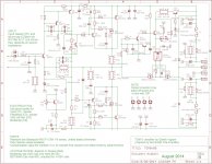
Hi zjjwwa...Would it be possible to post just that one Fig. 13.8. here? ...
Ah, OK. Thanks.
So the most "general" approach, where VbT need not necessarily be in relation to (or: equal to) Vb23 and / or Vb14. Kind of nice, because it allows to treat the two things totally independently.
As in: You could configure class B, cold class AB, or even hot class AB, and this would then be wholly independent of the amount of the VbT spread that you apply, between the cross-overs.
In this respect, I must admit, your approach to the implementation is rather clever.
But, if we resign from the EF Tripple, and a normal two-stage EF suffice, then theoretically, you could try the VbT == Vb23 == Vb14 ... But the standing currents would be significant then. I suppose it is indeed best if you have the freedom to keep/configure the VbT totally independently of Vb23 or Vb14.
Hi zjjwwa,
Have you run the spreadsheet?
In the ss you can change KbT -- which is VbT in units of Vt's (26mV). It is initially set at 3 (for 76mV). You can change any of the circuit values and see the new plots instantly. It gives exactly the same plots as LTspice.
Cheers,
Have you run the spreadsheet?
In the ss you can change KbT -- which is VbT in units of Vt's (26mV). It is initially set at 3 (for 76mV). You can change any of the circuit values and see the new plots instantly. It gives exactly the same plots as LTspice.
Cheers,
For class G, he states that it belongs to the classes which are combinations of transistors working in different classes, it is a B+C for a 2 rail voltages, and a B+C+C in 3 rail voltages.
Most class G (or H) amps cannot be considered clas AB+C. Why? Because the output is usually fed from the class AB stage all the time. It is the power supply (common terminal for AC signal) that is either modulated or switched. There have been a few exceptions that ARE class AB+C. Such amps have two (or 3) completely independent output stages which drive the load in parallel. The AB stage feeds the load until it’s supply runs out of voltage, then the class C stage takes over for output voltages above that. Probably the best example is the original QSC MX2000 (the non-A version). The component count was much higher - using two complete sets of D424/B554 per channel ($$$). Sounded better than the newer versions, too. It had that funky folded inside out common emitter output stage, but the same thing can be built with regular emitter followers.
It was a crazy weekend over here. But I promise that I will be looking into it on Monday evening.Hi zjjwwa,
Have you run the spreadsheet?
In the ss you can change KbT -- which is VbT in units of Vt's (26mV). It is initially set at 3 (for 76mV). You can change any of the circuit values and see the new plots instantly. It gives exactly the same plots as LTspice.
Cheers,
Classification concerns the transistors first. If a transistor leaves current passing for less than one alternance, it works in class C. There are transistors working in class C in a class G output stage.Most class G (or H) amps cannot be considered clas AB+C. Why? Because the output is usually fed from the class AB stage all the time. It is the power supply (common terminal for AC signal) that is either modulated or switched. There have been a few exceptions that ARE class AB+C. Such amps have two (or 3) completely independent output stages which drive the load in parallel. The AB stage feeds the load until it’s supply runs out of voltage, then the class C stage takes over for output voltages above that. Probably the best example is the original QSC MX2000 (the non-A version). The component count was much higher - using two complete sets of D424/B554 per channel ($$$). Sounded better than the newer versions, too. It had that funky folded inside out common emitter output stage, but the same thing can be built with regular emitter followers.
Their role is attached to the power supply of the optimised class B stage which is the only one "seen" by the load, unlike in the Quad current dumping stage where the load "sees" the class A and the class C devices in parallel.
Member
Joined 2009
Paid Member
In my TGM8 there is only one power rail and the Class AB is therefore in parallel with the Class C. It's not that the Class C stage takes over from the Class AB as the Class AB is always providing current to load when the Class C stage is active; what happens is that the Class C stage augments the Class AB stage above a certain current level. It has the great advantage that low signal levels we have the nice AB cross-over behaviour of a BJT transistor that requires relatively low idle current and then at high signals the Class C stage jumps in to help with powerful FETs. The power dissipation of the AB devices is capped and beta droop avoided. It sounds terrific.
Attachments
Similar in principle to a current shunt on a voltage regulator:In my TGM8...
Attachments
Last edited:
Yes. I played around with it a bit. Intriguing.Hi zjjwwa,
Have you run the spreadsheet?
Cheers,
OK. Some of the formulas - I do not fully understand, those with LN() operators, but I presume that there is some good established theory for them.
{Vk Vb Lekb Wekb Le2kb We2kb Io }
I assume that the formulas are OK and correct.
From here on, I played around with the parameters a bit.
I added some additional things.
From your AD column on sheet1, "Ie1234", I derived the following points:
(Start_X, Start_Y), (Stop_X, Stop_Y); Based on these two points, I calculated the slope and offset of a new set of values, for the AE column:
"SWWG" (as in Straight Wire With Gain).
In consecutive columns, I calculated the differences between the Straight Wire With Gain and your actual Ie1234 results. Then, I squared the differences. Then, totaled up the squared differences. For various scenarios: a). the whole range of input values, and b). for the critical center range of input voltage values, spanning from -0,1V do +0,1VFrom here on, I tried to find an optimal value for KbT. Indeed, there are certain minuscule deviations, slightly above 3,0 (3,05?) where I got smaller values of the sum of errors squared ... but from here on, I got confused with the results (sum of err squared vs. visual graphs).
Will be digging into it, maybe I will figure something out.
...
What keeps me perplexed and confused is the graph of Gm1234.
If it is the total resultant GM of the superposition of ALL transistors, ... and not just the anti-gm-doubling mechanism, then the "total gm" - should be a straight line. But it actually looks like the "anti-gm-doubling part" of the gm graph, the part that is to counter a classical AB stage with it's gm-doubling kinks.
But the "Gm1234" graph seems to already account for "ALL" of the transistors working in your scheme. So why the kinks in the Gm1234?
Or is this yet to be added to a traditional, AB class, with-gm-doubling stage in parallel?
- Status
- Not open for further replies.
- Home
- Amplifiers
- Solid State
- Class AB+C: Anybody tried it? Is it worth it?