Hi zjjwwa,
Good to see you are having some fun with the spreadsheet. There's a way to optimise in Excel using Solver. It is an add-in module that I used once (not sure if it's still supported). You set up an error measurement (like you did) and define boundaries for the parameters you want to vary using their algorithm to minimise your error value, then let it rip.
With this LTspice file you can step the parameters to optimise to get the best linearity in the "flat" gain region (I call the class-A region).
To understand the spreadsheet equations it would be best to start with the simple two transistor push-pull spreadsheet available here. There is a PDF explaining how it works here. Also read the preamble on my PAK website here PAK Project - PAK2 devo.
Cheers,
Good to see you are having some fun with the spreadsheet. There's a way to optimise in Excel using Solver. It is an add-in module that I used once (not sure if it's still supported). You set up an error measurement (like you did) and define boundaries for the parameters you want to vary using their algorithm to minimise your error value, then let it rip.
I confirmed the formulas are correct using LTspice circuit (download)I assume that the formulas are OK and correct.
With this LTspice file you can step the parameters to optimise to get the best linearity in the "flat" gain region (I call the class-A region).
To understand the spreadsheet equations it would be best to start with the simple two transistor push-pull spreadsheet available here. There is a PDF explaining how it works here. Also read the preamble on my PAK website here PAK Project - PAK2 devo.
Cheers,
Will start digging into these additional links / materials.Hi zjjwwa,
Good to see you are having some fun with the spreadsheet. There's a way to optimise in Excel using Solver. It is an add-in module that I used once (not sure if it's still supported). You set up an error measurement (like you did) and define boundaries for the parameters you want to vary using their algorithm to minimise your error value, then let it rip.
I confirmed the formulas are correct using LTspice circuit (download)
With this LTspice file you can step the parameters to optimise to get the best linearity in the "flat" gain region (I call the class-A region).
To understand the spreadsheet equations it would be best to start with the simple two transistor push-pull spreadsheet available here. There is a PDF explaining how it works here. Also read the preamble on my PAK website here PAK Project - PAK2 devo.
Cheers,
Hey, Ian, Your schematic, the one based on FAST configured drivers, it gives the fuzzy gut feeling that it should work OK. Work quite well, actually. Did you not ever feel the urge to actually build it and see how it sings?
{{ https://www.diyaudio.com/forums/att...tial-inputs-rush-vas-ops-only_05-jul-2018-png }}
Last edited:
Hey, Ian. Did you ever play "chicken"? Risky business ...Good to see you are having some fun with the spreadsheet.
Suppose that someone wants to build a practical circuit based on your schematic. One of the very first "challenges" that would come to mind is how to provide comfy stability to the pair of transistors that are sweating at quite a high standing current.
According to your wing-spread model, one pair of output devices (the "sleepers") are idling at a trickle of 3,5 mA, as calculated on your Sheet2. These - I would not worry about, for the time being.
But what worries me is the other pair of output devices (the "hard workers"), which even at idle conditions, are getting a beating with an idle current of 310mA. The first concern is: How does one ensure stability of this standing current, so that it does not wander off into thermal run-away and self destruction of the device(s)?
Did you do any sensitivity analysis for these devices, as to how stable is their standing current and what possible "thermal feedback" mechanisms could be put in place, so as to maintain optimal biasing, and guard against gross thermal run-away, as the temperature and associated Vbe changes unfavorably? For classical AB stages, a bias generator ... exists. So, there are known paths to pursue, such as putting the bias generator transistor in close thermal coupling with one of the output devices, plus possibly some additional tricks to ensure optimal biasing, for a wide range of operating temperatures.
But I can't even start to envision how one could ensure similar stability in your circuit. For starters ... it does not even include a bias spreader. So what would be the subject of "thermal stabilization"? The current sources/drains? But HOW? Putting the current source transistor on the heat sink - would actually be counter-productive: Higher temperature ==> lower Vbe ==> higher voltage drop on current-programming-emitter-resistor ==> higher current from the CCS ==> thermal runaway(?)
My assumption would be, that as the output devices get hotter, thermal stability would require that the CCS actually goes down with it's current. True? Maybe some form of "Differential CCS", where the "other" transistor is on the heat-sink?
A Penny for your Thoughts. How would you build it?
Could you put / add some real life implementation values to the resistors and rail voltages on your schematic?
If you were to apply some thermal/DC negative feedback just for the output stage, how would you do it?
Last edited:
Question: will this circuit work?
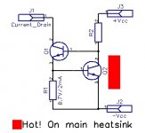
The goal is to create a pair of related (affinity, non-contesting) Thermally modulated Constant Current Source and Current Drain, exhibiting negative thermal feedback capability.
My idea being: The lower transistor Q3, mounted on main heat sink, will serve as a temperature sensor. Higher heat sink temperature shall reduce it's Vbe and hence reprogram the Constant Current Drain to a somewhat lower CCS current.
Lower Current Drain is actually comprised of a set of mirrored transistors Q1, Q2.
It is the sum of their currents that is held constant.
The upper side of the circuit is equipped with a current mirror, forcing equal currents through Q4, Q5. Instead of a third transistor, it is just two series connected diodes up there, to bias the bases. No transistor there, so as not to antagonize the Upper Source and the lower Drain. The upper "programming resistor" is just for the sake of symmetry. Does not perform any hard-core programming.
Will this work, as a means for additional thermal stability, in the context of Ian's double wing spread schematic?
Attachments

Last edited:
Hi zjjwwa,Will start digging into these additional links / materials.
Hey, Ian, Your schematic, the one based on FAST configured drivers, it gives the fuzzy gut feeling that it should work OK. Work quite well, actually. Did you not ever feel the urge to actually build it and see how it sings?
{{ https://www.diyaudio.com/forums/att...tial-inputs-rush-vas-ops-only_05-jul-2018-png }}
Yes, I wanted to build, but ... did you read my Rush pairs post?
As for its sound quality I stand by what I said in post 25
BTW I am interested in finding a better way to measure amplifier distortion than the standard THD measurements because, as you are probably aware, THD measurements do not correlate with sound quality. This has been known since D Massa's 1930 paper showed THD did not correlate to sound quality and he recommended that the use of THD for this reason "be discontinued". But no one did, probably because there wasn't anything else available (that worked) to replace it. So 90 years later we still have to listen to our amps to "see" how they sound. In the final analysis we have to disregard the THD measurements....Unfortunately there doesn't seem to be any finalized designs using Class-AB+C like Bob's DoubleCross or my CSD form --until there is the sonic advantages (if any) are guess work. I'm not in a position to help test one unfortunately.
How do you treat THD specs? Do you listen first then read the specs? There seems to be some justification for that approach.
Cheers,
Hi zjjwwa,Hey, Ian. Did you ever play "chicken"? Risky business ...
Suppose ...
A Penny for your Thoughts. How would you build it?...
Standard biasing can be used for this type of amplifier, eg Bob's DoubleCrossTM (aka Class-AB+C) since it is simply two standard output stages in parallel. Bob Cordell's gives several method for biasing his DoubleCrossTM (aka Class-AB+C) that he tested. Have you read it yet?
Biasing in my CSD Class-AB+C topology is a completely different approach since the power transistors are current driven and do not need a thermal bias loop to prevent thermal runaway. But the driver transistors need thermal compensation (mainly for ambient temperature changes).
My replies are delayed due to being in the Southern hemisphere (down under
 ).
).Cheers,
So sorry about that. Yes, I did read it, a few times actually, due to brain clipping overload, from the amount of new stuff and new ideas. I sort of missed out (or non-clicked), that detail that you not only simulated it, but also actually built it.Hi zjjwwa,
Yes, I wanted to build, but ... did you read my Rush pairs post?
As for its sound quality I stand by what I said in post 25
BTW I am interested in finding a better way to measure amplifier distortion than the standard THD measurements because, as you are probably aware, THD measurements do not correlate with sound quality. This has been known since D Massa's 1930 paper showed THD did not correlate to sound quality and he recommended that the use of THD for this reason "be discontinued". But no one did, probably because there wasn't anything else available (that worked) to replace it. So 90 years later we still have to listen to our amps to "see" how they sound. In the final analysis we have to disregard the THD measurements.
How do you treat THD specs? Do you listen first then read the specs? There seems to be some justification for that approach.
Cheers,
Would it be possible to apply your idea so as to create a Current Amplifier, with damping factor = 0 ?
I am aware of the THD paradox. Myself I have experiences with a cheerful 40kg DIY variation of the traditional Williamson, based on EL34, as well as a twice that much kg OTL, based on the MIG fighter jet tubes 6s33s. In both of the cases, THD is probably well over 1%, considering my unmatched resistors, capacitors, lousy output transformer (the first case), or the extreme abuse of the 6s33s (latter). In both cases, the sound is much more adorable than from many a commercial construct with much better published THD ratings. Yes, I listen, as opposed to measure. I know it very well that measurements (eg. PS Cables) do not always provide you with reasonable proof or explanations to what you hear. That is also the reason why I always insist that people first listen, before they judge.
I used to skip school, in Sydney, Australia, and run off with some Vegemite sandwiches to Bondi Beach to do some swimming, surfing, when I was a small kid.Hi zjjwwa,
Standard biasing can be used for this type of amplifier, eg Bob's DoubleCrossTM (aka Class-AB+C) since it is simply two standard output stages in parallel. Bob Cordell's gives several method for biasing his DoubleCrossTM (aka Class-AB+C) that he tested. Have you read it yet?
Biasing in my CSD Class-AB+C topology is a completely different approach since the power transistors are current driven and do not need a thermal bias loop to prevent thermal runaway. But the driver transistors need thermal compensation (mainly for ambient temperature changes).
My replies are delayed due to being in the Southern hemisphere (down under
Need to get that Book.
As for current driving of the driver stage and the output transistors, this is new stuff for me - still sleeping over it. Most probably, if there is a finite h21, and a finite supply of the base current, the output device standing current is probably also finite. But it is the thermal conditions and sensitivities that I am still trying to comprehend within such an approach.
Hi zjjwwa, ALL,...
As for current driving of the driver stage and the output transistors, this is new stuff for me - still sleeping over it. Most probably, if there is a finite h21, and a finite supply of the base current, the output device standing current is probably also finite. But it is the thermal conditions and sensitivities that I am still trying to comprehend within such an approach.
Attached is a snippet of my Linear Audio Vol.13 article to help explain it. Thermal sensitivity of the power transistor's idle current is less with current drive than the usual voltage drive. Also the crossover function (and hence optimal bias for minimum crossover distortion) is not affected to a first order approximation by temperature changes of the power transistors because crossover is done by the drivers.
Temperature increase of the power transistors increases the Beta (current gain) causing an overall gain increase which occurs relatively slowly -- it does not affect the optimum bias setting for the driver stage -- so there is no increase in crossover distortion when the power transistors heat up. My measurements showed this.
Cheers,
Attachments
Thank you for the link / literature. Digging into it.Hi zjjwwa, ALL,
Attached is a snippet of my Linear Audio Vol.13 article to help explain it. Thermal sensitivity of the power transistor's idle current is less with current drive than the usual voltage drive. Also the crossover function (and hence optimal bias for minimum crossover distortion) is not affected to a first order approximation by temperature changes of the power transistors because crossover is done by the drivers.
Temperature increase of the power transistors increases the Beta (current gain) causing an overall gain increase which occurs relatively slowly -- it does not affect the optimum bias setting for the driver stage -- so there is no increase in crossover distortion when the power transistors heat up. My measurements showed this.
Cheers,
Attached is the circuit for the article.Hi zjjwwa, ALL,
Attached is a snippet of my Linear Audio Vol.13 article to help explain it. ...
The above CSD amp circuit is from the PDF on How to set up the amp here.
There is also a lateral MOSFET version here.
Attachments
Last edited:
Thank you.Attached is the circuit for the article.
The above CSD amp circuit is from the PDF on How to set up the amp here.
There is also a lateral MOSFET version here.
Will be digging in. To the best of my ability.

- Status
- Not open for further replies.
- Home
- Amplifiers
- Solid State
- Class AB+C: Anybody tried it? Is it worth it?