Do you mean "Current Dumping" amplifier?edit: "FAST" ==> "Rush".
The output transistors are driven by a class AB Op Amp and the output transistors only switch on when needed.
That is the Quad 405. Have a look online at the schematics and training manual. You may find it answers a lot of questions for you.
~ QUAD 405 Amplifier Information and Modification ~
Will do. Thank you.Do you mean "Current Dumping" amplifier?
The output transistors are driven by a class AB Op Amp and the output transistors only switch on when needed.
That is the Quad 405. Have a look online at the schematics and training manual. You may find it answers a lot of questions for you.
~ QUAD 405 Amplifier Information and Modification ~
Looking into the workings of a Quad 405 is a noble task within itself.
Not sure, but I think that "Current Dumping" is a slightly different concept?
Is 'Current Dumping' based on the principle, that when one transistor is switching on, at exactly the same moment, a different transistor is switching off?
Last edited:
Indeed, checked after posting: Schottky.If you look at their type N°, you will see that the diodes of both examples are schottky
IIRC, I made a crude arithmetic estimation based on fixed voltages (300mV) and no internal resistance which I used in a sim, where I refined the values to take into account various real-life effect: junction equation, ohmic resistance, etc.
The values ended up rather low for the C branch, because the diodes have a non-negligible resistance of their own
Your comment on the non-negligible resistance of the diode itself is something that I did not consider. Thank you for the tip !!
Because it has no merit. All it does is create two hand-over points in the output current range. And it needs twice as many devices. And it wastes energy by running in class A....so why not give this concept a chance?
Hi zjjwwa,WHOAAA !!!!
...Was the "2:1" chosen arbitrarily, simply as a "conservative number" ? ...
Cheers, Ziggy.
Sorry if I freaked you out, apologies. Unfortunately there doesn't seem to be any finalized designs using Class-AB+C like Bob's DoubleCross or my CSD form --until there is the sonic advantages (if any) are guess work. I'm not in a position to help test one unfortunately. But I am willing to pass on all I know to anyone interested in designing one. Bob Cordell has built the output stage (only) for the standard topology and can probably answer queries better than I can on using it in a standard amp.
The link to my Rush pairs post has an example of compensation with a Class-AB+C output stage. It can be done safely.
As for the gain of 2 query for my CSD output stage. It was chosen to bring the voltage supply down on the VAS by half so standard 45V transistors can be used like the BC550/650. With selection for Vce you can have up to +/-50V power rails. After that, if you still want to use LV transistors, then bridge two amps takes you to 400W/8R - covering most DIYer's needs.
You probably think TO-92 or SOT-23 devices are too small for driving power transistors.😱 That is true in the standard topology. But for the CSD topology they can be used safely if done properly -- I have built and tested 2 versions with them: my Linear Audio CSD (Vol. 13) and Cube law (Vol. 8).
Cheers...
.
Last edited:
This link contains more details of how the Quad 405 works and of what it is capable of
Quad 405-2 upgrades
Stuart
Quad 405-2 upgrades
Stuart
Ian, Many Kind Thanks for your Inputs.Hi zjjwwa,
Sorry if I freaked you out, apologies. Unfortunately there doesn't seem to be any finalized designs using Class-AB+C like Bob's DoubleCross or my CSD form --until there is the sonic advantages (if any) are guess work. I'm not in a position to help test one unfortunately. But I am willing to pass on all I know to anyone interested in designing one. Bob Cordell has built the output stage (only) for the standard topology and can probably answer queries better than I can on using it in a standard amp.
The link to my Rush pairs post has an example of compensation with a Class-AB+C output stage. It can be done safely.
As for the gain of 2 query for my CSD output stage. It was chosen to bring the voltage supply down on the VAS by half so standard 45V transistors can be used like the BC550/650. With selection for Vce you can have up to +/-50V power rails. After that, if you still want to use LV transistors, then bridge two amps takes you to 400W/8R - covering most DIYer's needs.
You probably think TO-92 or SOT-23 devices are too small for driving power transistors.😱 That is true in the standard topology. But for the CSD topology they can be used safely if done properly -- I have built and tested 2 versions with them: my Linear Audio CSD (Vol. 13) and Cube law (Vol. 8).
heers...
.
The trick with the gain of 2 - very neat. Solves the problem of additional rails and steering far and clear from that additional complexity.
Started wondering about the thermal implications of the double bias generator connection (with two bias generators stacked on top of each other). This would undoubtedly result in the heat sinks running hot. Can't imagine it otherwise, if there will be a spread in the mid zone. It just hit me, that with two triplets, and 6 Vbe's on each, that would effectively translate to cross-over midpoints at +3Vbe and -3Vbe. That probably translates to 3x 0,7V = 2,1V.
I.e. cross-overs at +2,1V and at -2,1V. Now, i started thinking about the emitter resistors and the current that such voltage implies. Even if I go for 0,47R+0,47R metal plate, that is STILL less than one ohm, and hence standing current of probably 2,1/0,94 = 2,23 A of standing current per transistor (in the AB section). Basically, I can forget my 58V rails, because that would mean a crazy amount of idling watts. Probably could get away with the trick with lower rail voltage though.
Maybe, just maybe ... it would be a tad more doable, if it were not triplets, but 2-transistor EF's.
Then there would be just 2Vbe's in the midpoint, and the calculation would reduce to 2x0,7V/0,94R = 1,48 A. Now, this is a standing current, with which I could probably live with, provided that the rail voltages are reasonably low. (as in: much lower than 58V DC).
Anyways, there is still the alternative of going the easy route - i.e. reading the most trendy thread in the solid state section, and choosing PCB's purchase for one of the proven and documented designs, which can be found there. Such an option at least increases my chances that the DIY project will turn out successfully. The more I dig into the subject of building amplifiers, the more non obvious it all gets.
Tough call ...
Last edited:
Member
Joined 2009
Paid Member
Current dumping is a marketing term, the Quad was analysed by John Vanderkooy and Stanley Lipshitz many years ago and published in a seminal paper on feedforward in JAES.
Class AB+C could be used in a feedforward design but it's not the only option.
I used Class AB+C in a feedback design: TGM8 - an amplifier based on Rod Elliot P3a
Note: Rod Elliot did not use Class AB+C in his P3a, it was simply a starting point for my thread.
I had good reasons for using it and yes, it is worth it - depending on all the other details about your design.
The choose of this term has been somewhat criticized as being not very happy. I do not think it is unadapted. I have been looking for its meaning so I looked at its translation in french. A word fits quite well, translated back to english it gives : unballasting. In a circuit using current dumping, a stage having high current capabilities "assists", when needed, a stage having limited current capabilities, to deliver an intended current in a load.Current dumping is a marketing term.
Hi zjjwwa,Ian, Many Kind Thanks for your Inputs.
The trick with the gain of 2 - very neat. Solves the problem of additional rails and steering far and clear from that additional complexity.
Started wondering about the thermal implications of the double bias generator connection (with two bias generators stacked on top of each other). ....
...
Anyways, there is still the alternative of going the easy route - i.e. reading the most trendy thread in the solid state section, and choosing PCB's purchase for one of the proven and documented designs, which can be found there. Such an option at least increases my chances that the DIY project will turn out successfully. The more I dig into the subject of building amplifiers, the more non obvious it all gets.
Tough call ...
With Bob's an my implementation of Class-AB+C you don't have two Vbe bias generators "stacked on top of each other". The situation of Class-A bias is not as grim as suggested. Total idle current of 300mA for a 100W OPS can give a wide enough poser band to cover the 1st watt with negligible crossover distortion. That's not a lot of heat compared to standard Class-A amps and a lot less crossover distortion than standard Class-AB in optimum bias. And over the past decade there has been a move to paralleling Class-AB stages with minimal emitter resistors to get lower distortion and this is increasing the total idle current closer to 200mA for a 100W amp, so 300mA for Class-AB+C is no longer an issue, nor is the complexity with two parallel stages. The only difference is a few bias components.
This must be an improvement in the state of the art -- no development like this has been seen since the 1970's. BTW Quad "Current dumping" is different to Class-AB+C in that the latter does not need negative feedback whereas Quad's relies on negative feedback to form the balanced bridge so it iuses hybrid feedback plus feedforward. You can run my LTspice circuit for Class-AB+C operating as Common Emitter to see it can operate with zero feedback (apart from emitter degeneration). The file is available here. If you are not into LTspice then a spreadsheet showing the same is here. Screen shots are attached for both.
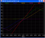
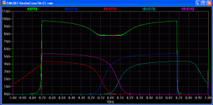
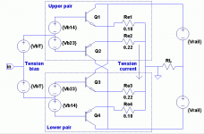
Now for biasing, look at the attached circuit based on Bob's book Figure 13.8a. Can you see two parallel output stages? The upper one is shifted up a small voltage by the "Tension" bias voltage and likewise the lower one is lowered. The plots for the currents show this shift. Bob says in his book the way to implement these bias voltages turns out to be surprisingly easy. I arrived at the same method independently. You may be able to see it in my circuit posted here, otherwise Bob's book gives a clearer implementation for implementing the bias generators than mine.
Re: building a successful design, there are presently no proven Class-AB+C projects. Bob Cordell has only built and tested the output stage. Bob is working on his BC-1 design out of his book and may be nearing the stage for DIYer's to make, see this post.
Re: digging into amplifiers -- they are very complex pieces of equipment, even the minimalist amps. The standard topology is the preferred one because it is the easiest one to get working and the best understood. When you get off that well worn track you can easily get lost in a jungle of complexity (like my amps😉). Even for the standard design you can spend a lifetime learning about it.
Cheers,
Attachments

Last edited:
The Quad 405 does not employ feed-forward. The intention was to eliminate the need for output stage bias current adjustment. So it has unbiased push-pull power transistors, class C if you like. The “missing” output current in the dead zone is supplied by a class A transconductance amp. This creates a problem of needing a very non-linear base voltage for the power transistors and the mitigation of this is done by the crafty balanced bridge.
This is not the same as the dual, class B push-pull being discussed here.
This is not the same as the dual, class B push-pull being discussed here.
How much current can the class A amp supply?The Quad 405 does not employ feed-forward. .... The “missing” output current in the dead zone is supplied by a class A transconductance amp. .
The class A part provides all the current across a centre dead zone of about 0.5-0.6V, double that in earlier models, so current = 0.6/8 or 0.6/4 or whatever your speaker impedance is. So 150mA into 4 ohms. The signal delivered to the power transistor bases is entertaining, especially Tr10. But it works, and works well.How much current can the class A amp supply?
Will need to catch up on a few things here, read up a bit.Hi zjjwwa,
With Bob's an my implementation of Class-AB+C you don't have two Vbe bias generators "stacked on top of each other". The situation of Class-A bias is not as grim as suggested. Total idle current of 300mA for a 100W OPS can give a wide enough poser band to cover the 1st watt with negligible crossover distortion. That's not a lot of heat compared to standard Class-A amps and a lot less crossover distortion than standard Class-AB in optimum bias. And over the past decade there has been a move to paralleling Class-AB stages with minimal emitter resistors to get lower distortion and this is increasing the total idle current closer to 200mA for a 100W amp, so 300mA for Class-AB+C is no longer an issue, nor is the complexity with two parallel stages. The only difference is a few bias components.
This must be an improvement in the state of the art -- no development like this has been seen since the 1970's. BTW Quad "Current dumping" is different to Class-AB+C in that the latter does not need negative feedback whereas Quad's relies on negative feedback to form the balanced bridge so it iuses hybrid feedback plus feedforward. You can run my LTspice circuit for Class-AB+C operating as Common Emitter to see it can operate with zero feedback (apart from emitter degeneration). The file is available here. If you are not into LTspice then a spreadsheet showing the same is here. Screen shots are attached for both.
Now for biasing, look at the attached circuit based on Bob's book Figure 13.8a. Can you see two parallel output stages? The upper one is shifted up a small voltage by the "Tension" bias voltage and likewise the lower one is lowered. The plots for the currents show this shift. Bob says in his book the way to implement these bias voltages turns out to be surprisingly easy. I arrived at the same method independently. You may be able to see it in my circuit posted here, otherwise Bob's book gives a clearer implementation for implementing the bias generators than mine.
Re: building a successful design, there are presently no proven Class-AB+C projects. Bob Cordell has only built and tested the output stage. Bob is working on his BC-1 design out of his book and may be nearing the stage for DIYer's to make, see this post.
Re: digging into amplifiers -- they are very complex pieces of equipment, even the minimalist amps. The standard topology is the preferred one because it is the easiest one to get working and the best understood. When you get off that well worn track you can easily get lost in a jungle of complexity (like my amps😉). Even for the standard design you can spend a lifetime learning about it.
Cheers,
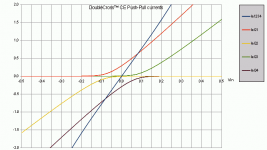
But basically, your graphs - look very familiar. To what I have been doing and plotting in excel at least. But using a more familiar, intuitive method.
The problem that I have with your circuit is that I need to better understand it first. It is in parts non-obvious ("exotic"?) to me. It seems to be achieving exactly the goal that I am looking for.
My 'more familiar' method was of the KISS variety, simple and stupid emitter resistors, which are bypassed by a diode and series connected similar, or better, slightly lower in value, resistors.
Picking specific proportions between them, and using a standing current of half the forward bias Vf of the diode used, seems to render similar results.
But at the same time - the rest of the circuit is "pretty much standard"....
Will need to think this over, the thing with your Rush transistors and how it works.
>>>> If you are not into LTspice then a spreadsheet showing the same is here.
Yes, I think that I will start off and dig into the xls sheet. More familiar.
>>> Bob's book ...
I do not have it yet. Would it be possible to post just that one Fig. 13.8. here?
...
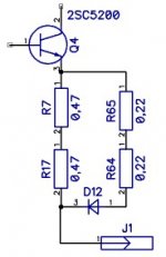
My "alternative method" - would be something crude and simple and stupid, but intuitively easy to embrace: The complex emitter resistor for the power devices. Practically, one would probably need to consider the internal impedance of the conducting diode, so my current pitch would be to lower the value of the diode bearing branch resistors to say 0R22+0R22.
I am actually soldering up a heat sink that will have the following emitter resistors now:
( 0R47 + 0R47) paralleled with ( 0,4_Forward_Voltage_Schottky_Diode + 0R22 + 0R22).
Optimum bias, according to my calculations, would be: 0,4V / 2 = 0,2V.
This allows for "equal distance" between the upper handover point (at 0,4V, start of diode conduction), and the lower handover point (transistor falls asleep).
The start of the of diode conduction, the total standing current would be:
a). Non-diode-bearing leg: 0,4V / 0R94 = 0,42A.
b). Diode-bearing leg: ... just starting to conduct here.
From a 58V rail, that would suggest 24,4 standing Watts per transistor, which I can live with.
Now, assuming some strong input signal, that increases the voltage on the complex emitter resistor to 1V:
a). Non-diode-bearing leg: 1V/0R94 = 1,06A
b). Diode-bearing leg: (1V-0,4V)/0R44 = 1,36A
Total: 2,42 A.
RMS Power on the 8 ohm load(?): 2,42 A * 2,42A * 8 ohms /2 = 23W
Peak voltage on 8 ohm load: 2,42A * 8 ohm = 19,4V
Power of the moment on the transistor: (58-19,4)*2,42 = 93 W, which it should handle (more or less).
I hope that I did not mix things up in this quick calculation.
At such strong signal condition, you can see that the proportion between currents: Diode-Bearing to Non-Diode-Bearing leg of the complex resistor is 1,36A / 1,06A = 1,28.
This proportion will gradually raise, as the signal gets stronger. A lucky coincidence, actually.
Because as current increases, I would assume that the h21 of the transistor decreases. But this actually coincides with gradually more and more current taking the now easier route via the 0R44 resistors (via diode), hence trans-conductance gradually increasing.
Does this rambling make any sense to you? What do you think?
Brutal Force. Simple and Stupid. But will it achieve the intended goal?
Yes, I think that I will start off and dig into the xls sheet. More familiar.
>>> Bob's book ...
I do not have it yet. Would it be possible to post just that one Fig. 13.8. here?
...
My "alternative method" - would be something crude and simple and stupid, but intuitively easy to embrace: The complex emitter resistor for the power devices. Practically, one would probably need to consider the internal impedance of the conducting diode, so my current pitch would be to lower the value of the diode bearing branch resistors to say 0R22+0R22.
I am actually soldering up a heat sink that will have the following emitter resistors now:
( 0R47 + 0R47) paralleled with ( 0,4_Forward_Voltage_Schottky_Diode + 0R22 + 0R22).
Optimum bias, according to my calculations, would be: 0,4V / 2 = 0,2V.
This allows for "equal distance" between the upper handover point (at 0,4V, start of diode conduction), and the lower handover point (transistor falls asleep).
The start of the of diode conduction, the total standing current would be:
a). Non-diode-bearing leg: 0,4V / 0R94 = 0,42A.
b). Diode-bearing leg: ... just starting to conduct here.
From a 58V rail, that would suggest 24,4 standing Watts per transistor, which I can live with.
Now, assuming some strong input signal, that increases the voltage on the complex emitter resistor to 1V:
a). Non-diode-bearing leg: 1V/0R94 = 1,06A
b). Diode-bearing leg: (1V-0,4V)/0R44 = 1,36A
Total: 2,42 A.
RMS Power on the 8 ohm load(?): 2,42 A * 2,42A * 8 ohms /2 = 23W
Peak voltage on 8 ohm load: 2,42A * 8 ohm = 19,4V
Power of the moment on the transistor: (58-19,4)*2,42 = 93 W, which it should handle (more or less).
I hope that I did not mix things up in this quick calculation.
At such strong signal condition, you can see that the proportion between currents: Diode-Bearing to Non-Diode-Bearing leg of the complex resistor is 1,36A / 1,06A = 1,28.
This proportion will gradually raise, as the signal gets stronger. A lucky coincidence, actually.
Because as current increases, I would assume that the h21 of the transistor decreases. But this actually coincides with gradually more and more current taking the now easier route via the 0R44 resistors (via diode), hence trans-conductance gradually increasing.
Does this rambling make any sense to you? What do you think?
Brutal Force. Simple and Stupid. But will it achieve the intended goal?
Attachments
Last edited:
The voltage drop 150mAx47 Ohm=7,05V, will it not open the output-stage long before? From were comes the 150mA during negative half-sine? Trough 2x560 Ohm from 50V supply? Please help a layman to understand.The class A part provides all the current across a centre dead zone of about 0.5-0.6V, double that in earlier models, so current = 0.6/8 or 0.6/4 or whatever your speaker impedance is. So 150mA into 4 ohms.
That's the voltage drop across the 47R resistor. I'm talking about the voltage drop across the load.The voltage drop 150mAx47 Ohm=7,05V, will it not open the output-stage long before? From were comes the 150mA during negative half-sine? Trough 2x560 Ohm from 50V supply? Please help a layman to understand.
Member
Joined 2009
Paid Member
The Quad 405 does not employ feed-forward.
A lot of people, like you, didn't understanding it properly until that paper was published from the University of Waterloo. I have a copy but was unable to upload it yesterday.
AES Journal Forum >> Feedforward Error Correction in Power Amplifiers
I do not see the class A stage as supplying the current in the dead zone of the class C stage. To me, the class C stage is supplying the major part of current when the class A stage can't provide it enough. Then both currents sum into the load. Maybe we can say that the class A commands and the class C obeys. All this is under the control of the balanced bridge which role is to obtain a constant output impedance, be the class C stage delivering current or not.The Quad 405 does not employ feed-forward. The intention was to eliminate the need for output stage bias current adjustment. So it has unbiased push-pull power transistors, class C if you like. The “missing” output current in the dead zone is supplied by a class A transconductance amp.
But this "class A current" (150mA) that causes that voltage drop across the load, from were does it come? Not trough the 47 ohm resistor?That's the voltage drop across the 47R resistor. I'm talking about the voltage drop across the load.
- Status
- Not open for further replies.
- Home
- Amplifiers
- Solid State
- Class AB+C: Anybody tried it? Is it worth it?