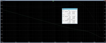
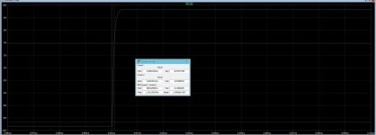
One more observation: just because amp works and plays music, it doesn't mean it's not oscillating. Many oscillations are not audible, or don't cause overheating (if not extreme), and are difficult to be seen on the oscilloscope....
of course. you reduce (global) negative feedback to get the amp stable.THD is considerably worse with cap in that place.
but I guess 0,00015% or 0,0005% (and even more) just sounds absolutely the same 🙂
Yep, that's the way it is.@minek123
What is more, THD is considerably worse with cap in that place.
The original circuit had THD 0.00015%
With 10pF the THD is 0.00050%.
With 22pF it is even more.
Stability comes at cost.
It's easy to design an excellent amp that is not stable.
But stability is importanter 🙂
That is comforting to know.of course. you reduce (global) negative feedback to get the amp stable.
but I guess 0,00015% or 0,0005% (and even more) just sounds absolutely the same 🙂
The sound stays practically the same.
No man alive has proven to hear THD 0.001%
Most opamp spice models are macro-models which are not very accurate in modeling distortions. So in practice THD of this amp may well be a decade worse than simulated.
how many gain we need ?Usually amp is considered being stable if PM is > 45 degrees.
Gain margin?
I would say around 10.
7-15 perhaps. Different people have different opinions on this..
I would say around 10.
7-15 perhaps. Different people have different opinions on this..
Here is the new Choctaw circuit. It is the 19th version I have in my computer!
New is the compensation cap 22pF to the opamp out.
I added also a cap across the feedback resistor 47pF.
This 47pF is to see as a lowpass filter. Reduces -3dB bandwidth to 200kHz.
Distortion simulated is THD 0.00093%
PhaseMargin is 76 Deg.
I hope this will be the Final circuit.
Oh, missing are the decoupling caps around the opamps supply rails. Two 100nF caps.
Last edited:
Great work, everyone.
I recommend adding 100nF caps, supply rails to ground, near the drains of the FETs. You're seeking low-inductance bypassing of the FETs, so this means short, heavy traces joining the drains, the two caps, and their path to ground. Surface mount parts will help by minimizing lead inductance.
I'll mention some general principles I'm sure everyone knows: increasing loop gain helps reduce distortion, and increased loop gain generally implies increased bandwidth. To that end, making the open loop bandwidth as large as practical helps, yielding more loop gain for distortion suppression. Obviously, the FETs are major players in this realm.
R1 and R2 help prevent local oscillation of the MOSFETs at very high frequency. The FETs have a lot of internal capacitance that combines with stray inductances to provoke oscillation. The gate resistors provide a lossy path to a low impedance node and de Q the resonances into stability. But the larger these resistors, the more the available gain-bandwidth is reduced. So careful compromise is beneficial.
In this circuit, the "low impedance node" alluded to above is the output of U1, so R3 and R4 are also part of the gate resistance paths. A remedy might be to shunt R3 and R4 with 100nF caps. Then you can trim bias currents and experiment with R1 and R2 independently. If you are able to extend OS bandwidth, you should see an improvement phase margin. Then you can reduce the opamp feedback capacitor and get reduced distortion.
I recommend watching this Bob Cordell seminar: #49 You may not have interest in his discussion of his amp, but in the later parts is invaluable advice on grounding/routing practice and component placement.
Another source I suggest: http://www.cordellaudio.com/papers/MOSFET_Power_Amp.pdf. This paper has sections on MOSFET oscillation and gate resistance.
Yet another: https://www.diyaudio.com/community/...ew-bjt-vs-mosfet.101745/page-156#post-7779163 This is a huge thread, but if you search for Bob's posts, you'll narrow the search and focus on the pertinent stuff relating to minimizing gate resistance. Within that thread you might also search for "Cgs".
Again, best to all.
Last edited:
I did a quick sim in LTSpice based on bohrok's sim, and there it is:
Thd: 0.0011% (really irrelevant...)
Estimated Slew Rate: 14V/us - more than enough for 10W amp.
Squares look perfect - but if someone plans to add RC filter at input, this would have to be re-simed with a specific filter.
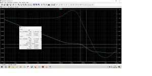
PM: 101, GM: 27 - somehow these numbers look 'too high', but maybe they are correct? No idea. Bottom line - I've never seen
numbers this high on any amp. If they are correct, that's great. Can someone verify this in LtSpice?
Basically they look like 'perfect' OLG plots for op-amp alone; we often see them is op-amp data sheets.
These numbers obviously differ from numbers reported by lineup (from multisim).
I used models for dual-die mosfets, and OPA model from TI.
Idle current little over 400mA.
Sim attached. Original Bohrok's sim didn't see op-amp model, so I had to change it a little bit.
Edit: One thing I would like see - in FFT profile - all harmonics under -120dB (non audible), but that's not going to happen on this kind of amp...
Attachments
I forgot that my opamp model was defined at OPA1656 symbol.Original Bohrok's sim didn't see op-amp model, so I had to change it a little bit.
You are using different mosfets (and models) but with those mosfets I get similar numbers with Tian probe: PM 95, GM 35.PM: 101, GM: 27 - somehow these numbers look 'too high', but maybe they are correct?
Yes. It's explained in the guide fir dummies mentioned by Zoltan
GM is too high, from what I know, gm higher than 15 is not desired. Not sure how critical this is...
Also - one more thing I just noticed: on my OLG plot, cursor2 is at 14MHz.
From what I remember, this is too high and may lead to instabilities, despite high PM numbers.
Desired frequency for the cursor2 should be below 5MHz. Perhaps someone more competent can confirm this?
That would also explain why these PM/GM numbers seem too high...
Last edited:
Not an expert on the matter, but nothing wrong with high gain margin. I have an amplifier with laterals that is unconditionally stable IRL with any capacitive load, from 100 pF to 10 uF, with or without any other load in parallel, and LTSpice calculates 55 dB gain margin.
I’m sure that many parasitic poles at very high frequencies make real plot somewhat different, but actual stability test is what matters the most.
So, don’t worry and carry on. 🙂

I’m sure that many parasitic poles at very high frequencies make real plot somewhat different, but actual stability test is what matters the most.
So, don’t worry and carry on. 🙂
Thd goes up because there is less open loop gain to correct the output fets.
Are those thd numbers taken under load?
Are those thd numbers taken under load?
Mine - yes. at full power.
But it's meaningless if op-amp is used. Most of op-amp models don't provide real-world Thd numbers (or data for thermal sims).
I'm not worried about Thd at all. This amp will have Thd as low as it gets in real world....
But it's meaningless if op-amp is used. Most of op-amp models don't provide real-world Thd numbers (or data for thermal sims).
I'm not worried about Thd at all. This amp will have Thd as low as it gets in real world....
Despite the new questions and doubts - I will build this amplifier
At most it will be a big BOOOOM 🤣
Yesterday I ordered 5 PCBs from JLCPCB
Today they are already on their way. They are fast!
I think they will reach me at the end of next week
As soon as they arrive - I will make a real prototype and check it
If everything is ok (especially stability -) )
I will have 4 boards left to take
Then I will also share the final version of Gerbers
- Home
- Amplifiers
- Solid State
- Choctaw - 10 Watt Amplifier, 1 Opamp + 2 MOSFET


