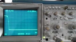
Here is a post showing measured edge rates on Quasimodo v.4. Rise time of the MOSFET gate is about 3 divisions at 10nsec/div. Fall time of the MOSFET drain (i.e. the "SCOPE" node) is about 1/3rd of a division at 10nsec/div. Cheapomodo is naturally expected to be worse, but not 200X worse.
How does the probe+vertical amplifier perform, when you feed it a really snappy square wave from a probe calibrator? The bandwidth - risetime equivalency formula (Wikipedia article here) says that a 100 MHz bandwidth probe+amplifier, ought to be able to display a waveform whose risetime is greater than or equal to 3.5 nanoseconds. Feed in an ideal perfect square wave with 1 picosecond rise time, and the 100 MHz scope+probe will display a 3.5ns risetime.
Wow the fall time on the Quasimodo is very quick. I would love to have a signal generator that could put out a perfect square wave with a 1 picosecond rise time, my signal generators are pretty bad by comparison. Also, the probe calibrator on my scope is useless, it only has a slew rate of about 2V/us.
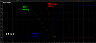
I've swapped the 5V supply for a 9V battery and probed about my circuit a bit and I think I've found that the cause of the sluggish behaviour is the output buffer.
The signal coming from the ne555 has a fall time of about 20ns but the signal measured at the output buffer has a fall time closer to 300ns.
The BS170 mosfets that I've used should have a turn-off time of 10ns, so I'm slightly puzzled as to what is causing the slow performance
Attachments

That's another I had not thought about..................I would profer that a test done on a transformer with a dual secondary used for full-wave rectification (as per typical HV B+ power supply in old valve amps), would best be done with the secondary 'not being tested' to be terminated with the target snubber - as that is the configuration being aimed for. There may be little difference between that non-tested secondary being shorted, and being terminated with a snubber, due to the component values in the snubber. ................
Determine the snubber for one secondary and fit it.
Then determine the snubber for the other secondary and fit it.
Then go back and check that the first snubber that was adopted is indeed correct when the other secondary is correctly terminated with a snubber.
That sounds right as a method.
What does it do to the tested secondary, when the other secondary is snubbered?
Don't forget that only one edge matters, the one where CheapoModo strikes the bell and makes it ring. That edge is:The signal coming from the ne555 has a fall time of about 20ns but the signal measured at the output buffer has a fall time closer to 300ns.
NE555 falling edge -> causes -> PNP BJT collector rising edge -> causes -> MOSFET drain falling edge.
The other edge is unimportant and can be made very leisurely. In fact it IS made very leisurely, to save DC power.In the quote above, you give a measured fall time at the PNP collector ("output buffer"). But what matters at the PNP collector is the rise time, not the fall time. Here it is, in simulation (below). You can really see the Miller effect, caused by the MOSFET's ((1+Av)*Cgd). They weren't lying to you in school; the Miller effect is not negligible.
And you do need to find a way to calibrate your probes & adjust their risetime-vs-overshoot trimmers for optimum performance. Otherwise your test instruments are lying to you. Nobody wants that!
_
Attachments
Last edited:
One way to get an answer is simulation. A second way to get an answer is to build a test jig on a protoboard / solderless breadboard, hook it up to a transformer and a dual trace oscilloscope, and observe. Configure your jig to provide whatever stimuli you think are important, and however many adjustable snubbers you deem necessary. A third way to get an answer is to connect your transformer in an actual power supply, with real diodes, real filter capacitors, real loads on the output, and adjustable snubbers. Then observe its behavior on a dual trace oscilloscope as you insert or remove snubbers, and as you adjust the snubbing resistances. A fourth way to get an answer is pencil and paper calculation, but this is messy because there are 3 coupled inductors and hence a 3x3 matrix of L's and M's. Me personally, I would not choose option four.What does it do to the tested secondary, when the other secondary is snubbered?
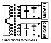
Make sure your configuration is NOT the independent dual secondary arrangement shown below. A quick way to check this is: if you've got less than two full bridges (fewer than 8 diodes total).
Independent dual secondaries, shown below, conduct at the same time and cease conducting at the same time. The diodes in the two bridges "ring the bell" of the secondaries' resonant circuits at the same time, and the snubbers damp the resonances at the same time. That's not the kind of behavior you and trobbins are interested in.
Attachments
Mark, it seems likely that with the two independent secondaries configuration, each with a bridge, the relevant diodes would only cease conducting at the same time if the secondary voltages, filter caps and loads on those two independent supplies were similar, given the subtle differences in diode conduction duration that may occur and the relatively short duration of diode turn-off.
Then you've just doubled your workload of things-to-be-tried, either on the bench, or in pencil-and-paper calculations, or in circuit simulation.
If you want to, you can double the work-to-be-done one more time, by including or excluding an "RRSF" after the snubber and before the rectifiers. This is a gizmo dreamed up by vacuum tube poweramp guys, called a Reverse Recovery Spike Filter. John "Buddha" Camille invented it and published it in the 03-1999 issue of VALVE magazine [archived online]. He felt that the enormous dV/dt's seen by the (solid state) rectifiers in a super high voltage power supply, gave rise to super high dI/dt's and hence, big reverse recovery spikes in the (1999 vintage) rectifier diodes. Claimed he saw big spikes on his scope. So he installed a slightly unorthodox 2R + 2C filter* between the rectifier and the snubber, to prevent the spikes from entering the transformer and reappearing on other windings. Lucky for you, his transformer had a center tapped secondary, i.e., two windings, thus your nervousness about multi winding secondaries applies here too. The RRSF idea became wildly popular in the "Bottlehead" chatrooms of AudioAsylum.com, with many people reporting huge sonic benefits after retrofitting an RRSF into their existing vacuum tube poweramp.
*he specified that the R's must be wirewound so they will include some inductance too
If improved awareness can be gained by working through different applications then that is a good adjunct to the tool imho. Clarifying what may be important to consider in certain circumstances, and when there are no practical implications, could assist those who just apply the tool but do no further in-situ testing.
It's likely that the default simplest Quasimodo test method, where all other windings are shorted, would result in the appropriate damped response when tested in situ for most circumstances. The interest I think now is in exploring whether there are certain situations which require any change in the test method.
Loudthud brought up Camille's "Development of a 211 Amplifier" article on music-electronics-forum, with bit of a chat ensuing.
It's a pity some images in old threads like http://www.diyaudio.com/forums/power-supplies/66542-fast-recovery-rectifier-diodes-10.html don't stand the test of time.
Last edited:
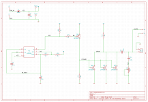
I finally received my sample pcbs. They have some practical issues because I used the default eagle libraries (thin pads etc) but it is functional.
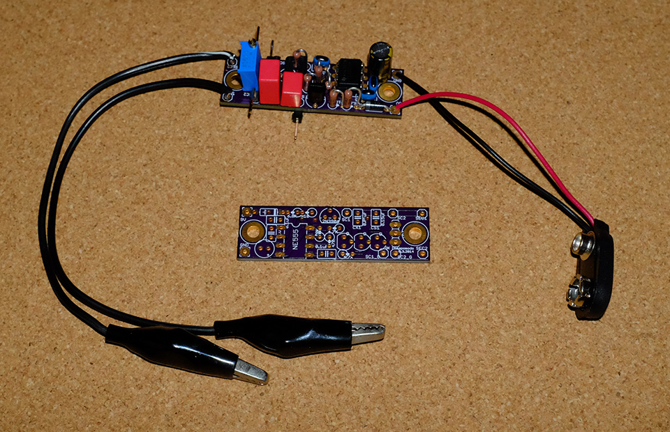
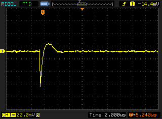
Here is a Triad 2x12VAC toroid ringing 🙂
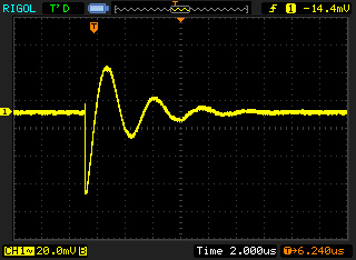
And here it is with the trimmer set at 47R7
Here is a Triad 2x12VAC toroid ringing 🙂
And here it is with the trimmer set at 47R7
Attachments


Congratulations on your working Cheapomodo! It looks like you've dialed in a resistor value that gives pretty good (zeta around 1.0) damping for that combination of transformer, Cx, and Cs. Nice job, well done.
I strongly recommend you try it again using two scope channels, one triggering on the near side of Cx (MOSFET drain) and the other displaying the far side of Cx (TRAFO secondary). The optimum snubbing resistor value won't change, but the scope's triggering and the display will be more solid.
By the way it appears you've got the 10X probe setting wrong somehow; the scope says your waveforms are millivolts tall, but a 9V battery + Cheapomodo produces waveforms that are several volts (several thousand millivolts) tall. And I think the "B" on your display might mean you ran the scope with Bandwidth Limit enabled; try not to do that, it distorts the sharp transients.
Thanks Mark
And again, thanks a lot for a very nice idea and circuit.
About the two channel triggering, if you check my layout, I have two sets of test points for two channels, as per your initial instructions. I just could not find a hook tip for the second probe. I've been using it mostly with the small spring.
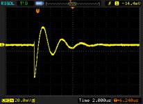
The small peak to peak voltage, could it be because I used AC coupling? So what we see here is just the ringing with no DC component? I run the probes at x1
About the bandwidth limit, I am usually too lazy to get my area clean enough from interference, so removing it results in a nasty thick spiky trace. Especially with the low resolution of the Rigol screen.
Anyway, the circuit idea is so nice that accurate measurements are not really required. All you have to do is hit auto and zoom until you see the ringing big enough to be easy and clear taming it.
And again, thanks a lot for a very nice idea and circuit.
About the two channel triggering, if you check my layout, I have two sets of test points for two channels, as per your initial instructions. I just could not find a hook tip for the second probe. I've been using it mostly with the small spring.
The small peak to peak voltage, could it be because I used AC coupling? So what we see here is just the ringing with no DC component? I run the probes at x1
About the bandwidth limit, I am usually too lazy to get my area clean enough from interference, so removing it results in a nasty thick spiky trace. Especially with the low resolution of the Rigol screen.
Anyway, the circuit idea is so nice that accurate measurements are not really required. All you have to do is hit auto and zoom until you see the ringing big enough to be easy and clear taming it.
Last edited:
I am starting an amp project so i decided to revisit this to measure a tranformer. I bought an Antek AN-5218 and with a 10nf Cx and 100nf Cs i twiddled the resistor pot i ended up with a figure of ~20ohms.
I did a quick search on the forum and found somebody else had measured the same transformer with a quasimodo and got (Cx - 0.01 uF, Cs - 0.15 uF, Rs - 170R).
There seems to be a large difference between 170R and 20R so did i mess up somewhere? I was testing with the primary wired for 240v and shorted out, and the other secondary winding shorted out (transformer has 2x 18v windings). I tried a few combinations like wiring the primary for 120v, paralleling the secondary's etc and never got a figure more than 40ohms. Any thoughts?
If I were you I would proceed systematically, step by step.
First I would measure Cx and Cs to 1% accuracy; if that is impossible or unacceptably expensive, I would purchase a few new Cx's and Cs's with tight tolerance from known-reliable suppliers, and verify that the known-correct-value Cx and Cs give R_snub_zeta1.00 = 20 ohms on my Antek AN-5218 transformer secondary.
Next I would use Cheapomodo to snub, not a transformer, but instead a fixed inductor whose inductance is known to within 5% (purchasing one if necessary). Does R_snub from Cheapomodo agree with Rsnub from mathematics, for this particular L-Cx resonant circuit?
At this point we know that Cx and Cs are as they should be, and that Cheapomodo tests are giving the correct Rsnub values which agree with 200 years of electrical engineering mathematics. The only thing to do now is to correctly attach the transformer secondary and correctly measure it with Cheapomodo.
If I continued to get R_snub_zeta1.00 = 20 ohms. I myself would conclude that this particular Antek AN-5218 transformer that I'm holding in my left hand, needs this particular CRC snubber that I'm holding in my right hand. If some other guy's transformer needs some other snubber, so be it. Maybe the secondary leakage inductance varies quite a lot from transformer to transformer. Maybe the other guy made mistakes. Maybe the other guy's transformer was defective. Maybe MY transformer is defective. Maybe the other guy was measuring an AN-0528 and typed the part number incorrectly.
I would find it highly significant, that THIS transformer here on my bench, coupled with THIS snubber here on my bench, gives THIS beautifully overdamped (zeta=1.0) waveform here on my scope. Unless I wired up my Cheapomodo test wrong and if I did, I deserve to suffer for it.
Thanks Mark. I have a cheap Capacitor/LCR meter that i used to verify the cap values so i am happy those are accurate.
I have a couple of inductors to hand from 100uh to large 10H, but unfortunately most of the Appendix A in your manual went right over my head so i'm at a loss on how to calculate the values manually.
My real problem is knowing if i should trust the board i built and the results i got without any verification of its accuracy. For example does 20ohms even sound like a plausible value, or is it way off the mark?
mcandmar,
Please see (post #487 of the Quasimodo thread). It shows one way to verify that your Cheapomodo is working properly.
Please see (post #487 of the Quasimodo thread). It shows one way to verify that your Cheapomodo is working properly.
Hi guys,
after spending ages trying to find a definitive (and simple) answer to calculate the effective RC values for the secondaries of my transformer and failing, this practical approach seems like an excellent solution 🙂
Does anyone have boards currently available and if not, what's the latest and greatest version of the files if I wanted to get some produced?
cheers,
James
CheapoModo is very small and has few easily available components, that it can be assembled on Vero board, or on plug board, or Proto board, or dead bug style, that you don't need a PCB.
Thanks Andrew,CheapoModo is very small and has few easily available components, that it can be assembled on Vero board, or on plug board, or Proto board, or dead bug style, that you don't need a PCB.
I'll have a go at making something up 🙂
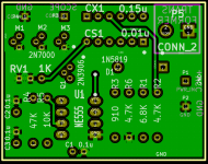
I built two revs of PCB for CheapoModo at seeed, using their cheapest-of-all footprint, 5cm x 5cm.
The second rev is shown below; its MOSFET gate driver is a wildly asymmetric PNP-resistor stage, giving one sharp edge (the falling edge), and one very sloppy and leisurely edge (the other one). Fortunately this does not matter since we set the scope to trigger on the falling edge.
Bypass capacitance was severely compromised; there's only a single capacitor for the whole board, compared to Quasimodo with a big electrolytic bulk capacitor plus many ceramic HF decouplers. Nevertheless it seems to work moderately well.
I have a supply of ~5 blank boards somewhere, stored in one of ~300 cardboard moving boxes in my garage. I will give one board to you free, IF you'll pay me $5000 to unpack those boxes and locate the boards 🙂
Otherwise here is a zip archive of the PCB Gerber files, which you can send to a board house yourself. Or design your own, as intrepid diyAudio member dimkasta did in (post #68 of this thread). You'll have more fun and learn more, too!
edit- and for those who can't resist using hod rod parts to produce a little extra horsepower (enabling the macho boast "Mine is bigger than yours!"), have a look at post #37 of this thread.
_
Attachments

Last edited:
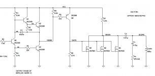
Remind me please.
The "kick", or step change impulse, to instigate the ringing is to pull current/charge from the output capacitor Cx1.
The Rds on of the 2n7000 in parallel needs to be low to allow a high current to flow to ground to discharge Cx1.
To get that fast "kick" Q1 needs to pull the gates of the paralleled 2n7000 high.
Is that correct?
How long do the FET Gates need to be held high?
- Home
- Amplifiers
- Power Supplies
- CheapoModo: quick and dirty transformer snubber bellringer jig