Thanks juma, I had played with a simplified version of this back in post #10. Its a neat circuit, no question, the only downside is the need for a trimmer (or two!) to null the offset.
You're quite right juma - your circuit fulfils all the criteria at #1. Its an interesting circuit, thanks for sharing.
Member
Joined 2009
Paid Member
Hi,
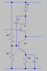
apart from the trimpot P1 the circuit in #7 fulfills all Your requirements a), b) and c), its even pushpull 😉
When using thermally coupled JFETs (or Duals) thermal stability -and thermally related offset drift- is also low.
You could then omit with the trimpot and install a fixed trimmer-R instead .... or a large output coupling cap 😉
jauu
Calvin
Does the connection labelled "d2a" make this a push pull topology?Hi,
apart from the trimpot P1 the circuit in #7 fulfills all Your requirements a), b) and c), its even pushpull 😉
When using thermally coupled JFETs (or Duals) thermal stability -and thermally related offset drift- is also low.
You could then omit with the trimpot and install a fixed trimmer-R instead .... or a large output coupling cap 😉
jauu
Calvin
Hi,
yes, the current source towards the negative supply is modulated by the voltage drop over R15.
Its a SEPP (Single Ended Push Pull) topology.
As such Class-A biasing is required.
The current swings will not be perfectly symmetrical in amplitude, but the current source will supply for a considerable part of the load signal current.
The Buffer can drive lower impedances with lower distortions for the same set idle current than with a unmodulated ccs.
jauu
Calvin
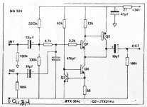
Using a JFET instead of a BJT at the input raises Zin and gets you rid of DC offset at the input and the output. BF862 is current production, high gm, low noise JFET. The buffer in attachment will effortlessly drive 2V RMS into 1k pot.
R2 will depend on your JFET's Idss and can be in range from 4R7 to 10R (right value will set your output DC offset at few mV and with P1 you can trim it down to zero).
CCS BJT will dissipate about 200mW so if you feel uncomfortable with it, use higher power device (BD139 or similar). Power consumption is about 20mA per rail, per channel.
Power rail voltage can be lowered by using a RC cells followed by 7x12 regs (or any other 10-12V regs of your choice).
What is the output impedance of this circuit juma? have you measured it?
Cheers George
Attachments

Last edited:
I don't have the prototype any more but my notes say:
Zout ~ 2 Ohms
Nice and low, thanks.
Btw did you ever makes some pcb boards for this?
Cheers George
No, it's too simple and small for a "real" PCB. Perfboard and p2p are OK for such a simple circuit.
Not exactly related to this thread, but FWIW I've found a way to make a SEPP with much larger peak current than 2x the standing current (more like a 10:1 ratio) which still remains in Class-A operation (no turn-off). Useful for low power circuits, at some 100uA total consumption it can handle occasional 1mA peak currents with grace.yes, the current source towards the negative supply is modulated by the voltage drop over R15.
Its a SEPP (Single Ended Push Pull) topology.
As such Class-A biasing is required.
Conceptual schematic below, the sensing resistor is replaced by a diode which did the trick.
Attachments
No, it's too simple and small for a "real" PCB. Perfboard and p2p are OK for such a simple circuit.
Cheers, I'll just p2p it when I get around to doing it. What sort of input can it take before getting troubled?
Cheers George
George
3V into 1k and 2V into 600R is what I tested as OK. It is voltage/current/load dependent.
3V into 1k and 2V into 600R is what I tested as OK. It is voltage/current/load dependent.
http://cds.linear.com/docs/en/datasheet/1363fa.pdfEdit; see post #11 for information about modern op amps capable of driving a 1k pot to line levels.
http://cds.linear.com/docs/en/datasheet/18189fb.pdf
Using a JFET instead of a BJT at the input raises Zin and gets you rid of DC offset at the input and the output. BF862 is current production, high gm, low noise JFET. The buffer in attachment will effortlessly drive 2V RMS into 1k pot.
R2 will depend on your JFET's Idss and can be in range from 4R7 to 10R (right value will set your output DC offset at few mV and with P1 you can trim it down to zero).
CCS BJT will dissipate about 200mW so if you feel uncomfortable with it, use higher power device (BD139 or similar). Power consumption is about 20mA per rail, per channel.
Power rail voltage can be lowered by using a RC cells followed by 7x12 regs (or any other 10-12V regs of your choice).
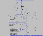
Juma,
what is your experience with the gate leakage of the BF862?
If - in a similar, non CFP configuration - I wire the gate of the BF862 to a volume pot, it will drive the output DC up and down by some mV.
DC leakage in bf862 depends on Vds. Keep it as low as you can - the gate to GND resistor too. Cascoding keeps the Vds low and stable.
If you know what are you doing it's a non-issue.
If you know what are you doing it's a non-issue.
- Home
- Source & Line
- Analog Line Level
- CFP Unity Gain Buffer