That does not help in getting any closer to confirming the Vgs of the device.A master of simple arithmetics shouldn't have a problem with such a trivial calculation.
Hi,
yes, Vds= Vdg+Vgs ... since Vgs is negative for n-channel JFETs -or in other words: the Source is more positive than the Gate- is the Vds smaller in Value than Vdg.
Keep in mind that Vgs only equals Vgate when there´s no source resistor -in that case Vgs=0 and Id=Idss.
If there´s a source resistor than Vgate equals Vgs + V(Rs) .. with V(Rs)=Id x Rs
As under normal conditions the Gate leakage is extremely small, the voltage drop over the gate resistor is typically negligable.
For circuit analysis one can assume the gate resistor as non-existant, i.e. replace it by a short.
Regarding the fig.9 You could supply a current through a ccs and vary the Vdg (or Vds) of the BF862.
jauu
Calvin
No free answers for trolls. You'll get the answer after showing a receipt for 50 GBP donation to the forum.That does not help in getting any closer to confirming the Vgs of the device.
Regarding the fig.9 You could supply a current through a ccs and vary the Vdg (or Vds) of the BF862.
my problem with fig 9 is that I can fix Id and Vdg or Vds. Fig 9 claims it can fix all three. Is this a typo?
I assume, that Your test conditions may already have lead to a latch-up or had come close enough that You could measure considerable gate voltage levels.
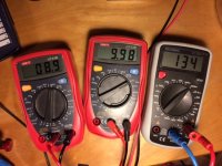
OK, different device: Idss 18.3 @ 8V Vds.
Setup as Juma's, 10 Ohm source to Vneg, 100kOhm gate to Vneg, drain to Vpos.
Left to right V(100kOhm) = 8.9mV, Vds = 9.98V, V(10Ohm)=134mV
Face it, this is real, my batch doesn't handle 10V very well.
Attachments
The hybrid CFP buffer proposed by Juma simulates also quite nicely when adding a drain resistor.


The benefit of this resistor is a lower Vds on the jfet to avoid gate leakage.
A constant Vds can be had with a bjt cascode.


Comments welcome.
The benefit of this resistor is a lower Vds on the jfet to avoid gate leakage.
A constant Vds can be had with a bjt cascode.
Comments welcome.
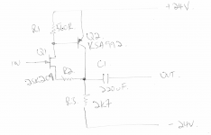
Apologies for resurrecting an old thread, but I'm considering incorporating a hybrid jfet / bjt CFP buffer into a new project. Essentially I am looking for a buffer circuit to interpose between a 4051 logic IC used for channel switching and the volume and balance pots. My requirements this time around are a little different to those at post #1:
- Very high input impedance to minimise the voltage across the non-linear series resistance of the 4051 IC, hence the jfet input.
- Sufficient current handling to drive ~2Vrms through the 10k volume and balance pots. PA input impedance approx. ~22k.
- Supply voltages are well-regulated +/- 24V, derived from the main PA rails (+/- 56V).
The 2SK209 fet looks to be a reasonable choice as the low Idss version (Y grade = 1.2 - 3.0 mA) is readily available and it has a high breakdown voltage for a jfet.
Rough sketch of the buffer stage below:
- The fet current setting resistor (R1) is chosen to supply ~1mA, which is just below the minimum for the 2SK209 in the Y grade range.
- R2 is chosen experimentally to minimise DC offset at Q2 collector. The output cap will ensure there is no DC across the pot track ends. Question: is there any need for R2 if the cap is installed?
Also interested in peoples practical experience stabilising this circuit. In my own experience with all-bjt CFP buffers, an input R on the order of 1k and a 10-22pF across the B-C junction of the master-bjt are required to prevent oscillation in the mhz region.
Attachments
Hey guys, I hate to be a nag, but it would be great if someone could share their tips on how to stabilise this hybrid fet cfp circuit.
Method 1: put a ferrite bead on the JFET source (where R2 is in post #68), to increase its impedance at the localized frequencies where ringing / oscillation is occurring. Don't bother putting ferrite beads on the BJT collector, as this is already high impedance and will benefit much less (if at all).
Method 2: add a base resistor to the BJT, relocate the loading resistor (R1 in the post #68 drawing) to between the BJT base and emitter, and insert a small-value capacitor (less than 100pF should do) across the BJT base and collector.
Method 3: add a small value capacitor (less than 100pF should do) from the gate of Q1, either to the drain or ground.
Finally, compact construction matters, especially when working with gates and bases. Minimizing the lengths of gate and base leads / PCB traces is recommended.
kr, jonathan
Hey guys, I hate to be a nag, but it would be great if someone could share their tips on how to stabilise this hybrid fet cfp circuit.
You could run it through LTspice, that's normally very good at unearthing any stability issues.
Jan
Jan, not necessarily. Physical construction can have an impact on circuit stability / performance, an aspect which will not appear in a simulator.
Excess lead length can spell the difference between a circuit that oscillates, is stable, or is stable but readily perturbed by RF.
Excess lead length can spell the difference between a circuit that oscillates, is stable, or is stable but readily perturbed by RF.
- Home
- Source & Line
- Analog Line Level
- CFP Unity Gain Buffer