Ian,
Try putting in a 10-22 ohm resistor on the emitter of the cfp master, between the emitter and the drain of the mosfet.
This will reduce cfp open loop gain, improving stability margin, and is a well tried technique suggested by Self, amongst others.
I've also found that the speed of the master should be at least three times the speed of the slave. This puts quite a spec on the bipolar driver, so it should be around 200MHz at least.
Driver degeneration will degrade feedback factor, but it will still perform well.....
Cheers,
Hugh
That's better.
Where, physically, is the zobel (RC shunt) for the output? What are its values and where does it connect to gnd?
1m for each psu wire is TOO MUCH. You want to get the length below 30cm and you need to minimize the loop areas by cable tying the wires together.
You should have 4 psu wires leaving the pcb.
1. plus V
2. neg V
3. input ground (R1, C7, R12, R14, phono coax shield)
4. Zobel ground
The phono connector should not be connected to the amp ground by any other path, eg: by the case (if you have a case yet)
Did you say that the local decouplers on the pcb are not installed? If not, you should short out R36.
Before we start modifying the circuit dynamic response, let's check you have the basics right.
1) Zobel?
2) short R36 (as I said before)
3) The bottom of C8 is connected to the wrong side of VR3.
4) What is R16 for? Short it out.
5) There is nothing to reduce RF pick-up at the input. R1 should have a 470pF to 1nF cap across it, and you should have a series resistor between C2 and R1 of 2k or so.
Once you've made these mods and sorted your wiring out, please report on the frequency of the oscillation. Then we'll go through simple steps to stop it oscillating.
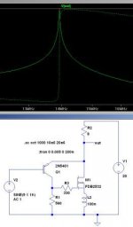
This is to illustrate my previous comment about the intrisic instability of the topology by itself:
The simulation shows the frequency response of such a composite. The transistors, values and parasitics are different from those of the amplifier, but they would mainly influence the frequency and strength of oscillations.
The screenshot shows a peak of 54dB in the gain at about 14MHz. Not too bad for unity gain buffer!
In practice, this simply means it will oscillate at this frequency.
Attachments
Just logged on and this caught my eye, not read the other responses yet.ian_elvar said:
The sim shows 8mA through the driver stage with the 560's. Going down to 100 will yield 50mA, and obviously anything in between.
8mA and 560r =4.48V across the gate/source of a Lateral FET.
This is bonkers.
If the sim is predicting 4.48Vgs then go and look at the datasheet graphs and you will see it is telling you lies. Either you have set up the sim wrongly or the LFET model is actually a vFET.
Measure the circuit gate/source voltage and measure the 560r volts drop.
Good morning. I've just picked up you replies, but I'm off to work in a moment.
Traderbam - Zobel is between the 5W resistors, mounted copper side. You should be able to see it on the PCB. It has its own ground. R36 is already shorted, sorry I forgot to update that one the scm. I'll make the wiring mods and IP filter later and report back.
Elvee - I see your point. Now I guess the big question is how do we manipulate it to work in a stable fashion? I'll set the same circuit up in the sim and have a play around.
AKSA - I'll have a go at your suggestions after I've completed the above. I wondered about doing something like that myself
Andrew - Yes, it seems a bit weird. I forgot to measure the voltage across them in the real circuit last night, but I'll make sure I do later on and let you know.
There's got to be an answer to all this - that's half the fun of doing it 🙂 Thanks for all your continued help
6mA through R10 @47r is too high a volts drop.
The protection transistor will start to turn on @ ~ 400mV, that's 8.5mA.
You must lower R10 or split it, to ensure the quiescent voltage on the protection base/emitter is below 200mV and preferably ~150mV. This allows the VAS current to swing either side of the 6mA quiescent current and for the protection to not trigger.
At the moment with VR for the CCS set points you cannot measure the actual quiescent currents. How do you know that the circuit is doing what the sim predicts and what you would expect?
Measure every current, that you can (Vacross resistor), on the PCB and plot them on your schematic.
Go back to the sim and ask it to display all these currents and plot them in a different colour. Now examine what the circuit is doing.
Hi Elvee,
re post 24,
what does AKSA's 10r to 22r in the emitter lead do for the oscillation?
What other components stabilise this topology?
Does adding a bit of nH to the gate make the problem worse?
re post 24,
what does AKSA's 10r to 22r in the emitter lead do for the oscillation?
What other components stabilise this topology?
Does adding a bit of nH to the gate make the problem worse?
Andrew,
According to the MagnaTEC datasheets, the Vgs threshold will be between 0.1V and 1.5V. So the values of R22 and R23 are hard to determine without measuring the actual transistors being used, as you have asked. Best if Ian can find two parts with similar Vgsth and above 1V.
The stability of the CFB outputs are one of the 7 issues I identified earlier. The optimum values of gate and driver emitter resistors will depend upon the values of R22 and R23, and will be different for each phase.
So I recommend Ian gets the dc operating points and R22 and R23 values finalized before we recommend frequency compensation components.
Brian
I have Source follwer outputs in my 1058/162 output stage.traderbam said:According to the MagnaTEC datasheets, the Vgs threshold will be between 0.1V and 1.5V. So the values of R22 and R23 are hard to determine without measuring the actual transistors being used, as you have asked. Best if Ian can find two parts with similar Vgsth and above 1V.
Vgs~550mV for 75mA output bias. i.e. 1.1V across BOTH gate to gate pins of the SF pair.
The Magna should be within the range specified. Not ~4.5Vgs.
Presumably, the internal diode would prevent inverted connection (S to D) of the FETs????
AndrewT said:I have Source follwer outputs in my 1058/162 output stage.
Vgs~550mV for 75mA output bias. i.e. 1.1V across BOTH gate to gate pins of the SF pair.
The Magna should be within the range specified. Not ~4.5Vgs.
Presumably, the internal diode would prevent inverted connection (S to D) of the FETs????
Very good point, Andrew. That low a Vgs is not going to work for Ian unless he replaces R22 & R23 with CCS, but this will get complicated because a CCS will need >1V across it. There simply won't be enough driver current range to drive the FETs, otherwise.
What would you recommend Ian does about this problem?
I can't comment on the internal diode. It probably won't survive much If.
r22 has Vgs across it.
If Vgs=1V then 220r has 4.5mA passing to the driver.
Now adjust the driver current very slightly and the Collector current varies slightly. This tiny variation is sensed by the G/S and varies the current passing the FET.
It works IF THE PEAKING identified by Elvee can be eliminated.
Measure the Vgs and then select r22. But he did that before he selected his FETs for assembly. or didn't he?
What speed does the datasheet show for the s1381 @ Ic = 1mA to 5mA?
I think there is no design, based on informed decision making, in this amp.
It's bits banged together and hope.
BTW.
D.Self explains in detail the purpose of R16. Leave it in place.
R16=18r better suits CCS=7mA.
what is CCS value?
AndrewT said:Hi Elvee,
re post 24,
what does AKSA's 10r to 22r in the emitter lead do for the oscillation?
What other components stabilise this topology?
Does adding a bit of nH to the gate make the problem worse?
15r in the emitter cures the problem completely with this particular configuration.
There just remains a small gain hump of 0.5dB at ~4.6MHz
It would be dangerous however to draw general conclusions: for example, without the emitter resistor, any inductance in the drain lead tends to damp the oscillatory behaviour. When the resistor is present, a drain inductance of 100nH increases the 4.6MHz hump to 2dB. Not catastrophic yet, but it shows all elements interact, and a good solution in one case might actually make things worse in another.
This why this topology is so difficult : you cannot apply one-size-fits-all strategies.
Adding 100nH in the gate decreases the gain peak from 54 to 32dB. It thus seems to improve the stability, but once again with all caveats applying.
Hi Elvee,
thanks for taking the time to do that for us.
What effect would a low inductance decoupling cap on the FET have?
Could you post the input data for these sims?
thanks for taking the time to do that for us.
What effect would a low inductance decoupling cap on the FET have?
Could you post the input data for these sims?
Kiss of deathAndrewT said:BTW.
D.Self explains in detail the purpose of R16. Leave it in place.
R16=18r better suits CCS=7mA.
what is CCS value?

Where does he explain this?
it's Vbe multiplier analysis and trying to minimise the drift in Vbe voltage as the VAS swings current around it's quiescent value.
As a result of his stating and proving that Vq is the critical parameter for minimum distortion in an optimised ClassAB (=Self's ClassB), it follows that stability in the Vbe multiplier voltage is essential to closely maintaining Vq.
fig6.17 in "the output stageII" of edition 2 of audio amplifier design handbook. But also on his web site.
Ok, thanks Andrew. I gather R16 tries to compensate for the effective series resistance of the virtual battery. Small effect.
My designs do not use this topology so I haven't analyzed this circuit in detail.
My designs do not use this topology so I haven't analyzed this circuit in detail.
AndrewT said:What speed does the datasheet show for the s1381 @ Ic = 1mA to 5mA?
Look it up here: Datasheet Catalog
I suppose you mean across the supply. In this case, it is not needed, because the simulator assumes a zero impedance for voltage sources, unless a value is defined.AndrewT said:Hi Elvee,
thanks for taking the time to do that for us.
What effect would a low inductance decoupling cap on the FET have?
If a 100nH inductance is added, to simulate a non-perfect decoupling, the gain peak falls to 6dB. Again, a somewhat surprising and anti-intuitive result.
I don't see what you mean. All the data are on the schematic, and the simulation is an AC analysis of the gain and phase vs frequency, between the input voltage/bias source and the output node.Could you post the input data for these sims?
- Status
- Not open for further replies.
- Home
- Amplifiers
- Solid State
- CFP oscillation woes