Yes X,just stil working on it!Hi Thimios,
You must be exhausted from working on this amp non stop and now taking a break. Take your time - just wondering what we need to do to implant the fixes.
Thanks again.
X
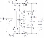
The first critical modifications is to leave these C14,C16 positions empty.
Νow simply playing with different VAS current to see what is better.
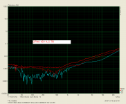
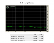
I see a little higher distortion in the high frequency area.
Maybe Shaan or Valery can help.
Attachments
Last edited:
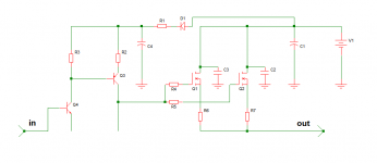
This config has consistently given me good results.
Showing only the positive rail.
The negative is the same, only capacitor/diode polarity reversed.
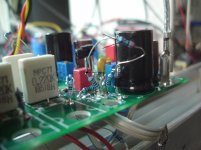
C1= 100uF (right after PS input).
C2,C3= 100nF (as close as possible to drain pin of MOSFETs).
D1=1N4007 (powered with separate trace from C1, with a close-by ground trace from PS ground to connect C2,C3,C4).
R1= 10R.
C4=220uF (VAS and input powered right from C4 supply pin).
Hope this helps in future designs.
Showing only the positive rail.
The negative is the same, only capacitor/diode polarity reversed.
C1= 100uF (right after PS input).
C2,C3= 100nF (as close as possible to drain pin of MOSFETs).
D1=1N4007 (powered with separate trace from C1, with a close-by ground trace from PS ground to connect C2,C3,C4).
R1= 10R.
C4=220uF (VAS and input powered right from C4 supply pin).
Hope this helps in future designs.
Attachments
R2=?what about VAS current?This config has consistently given me good results.
Showing only the positive rail.
The negative is the same, only capacitor/diode polarity reversed.
C1= 100uF (right after PS input).
C2,C3= 100nF (as close as possible to drain pin of MOSFETs).
D1=1N4007 (powered with separate trace from C1, with a close-by ground trace from PS ground to connect C2,C3,C4).
R1= 10R.
C4=220uF (VAS and input powered right from C4 supply pin).
Hope this helps in future designs.
post782 describes well what one needs to do, to layout the local supply rail decoupling.
Note the statement
Layout design is not about making it look aesthetically pleasing, it is about getting the currents to follow the desired routes that maximises circuit performance.
Note the statement
This is the decoupling ground. It is where the half sinewaves going to the output get resolved.with a close-by ground trace from PS ground to connect C2,C3,C4
Layout design is not about making it look aesthetically pleasing, it is about getting the currents to follow the desired routes that maximises circuit performance.
Last edited:
R2=?what about VAS current?
The 15k/18k resistor that will feed the NPN input BJT's emitter will control PNP VAS current and it is taken from negative supply. Yes it would be wise to connect that resistor right to C4's supply pin as well, but to the C4 of the negative rail. 🙂
Yes X,just stil working on it!
The first critical modifications is to leave these C14,C16 positions empty.
Νow simply playing with different VAS current to see what is better.
I see a little higher distortion in the high frequency area.
Maybe Shaan or Valery can help.
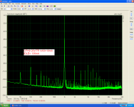
Try running 150mA to 180mA bias (ea MOSFET) on the outputs and see if that helps. I did not notice rising distortion at the speaker - which natively have -50dB THD.
R2=?what about VAS current?
Do not increase R2 above 10R. Control VAS current by increasing the 15K resistors to like 18K.

Ok,so increasing the 15K up to see 150mV on R7(10R)
Attachments
Last edited:
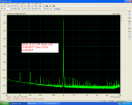
Ok,so increasing the 15K up to see 150mV on R7(10R)
Yes.
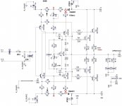
Cut the two crossed points and join the 10R VAS resistors to A and B points of each rail. Decouple A and B points with 100uF or 220uF.
Attachments
Last edited:

Was it the fact that the original power rail caps were improperly grounded or because they were so big (4700uF) that caused problems by allowing a low frequency ground loop to form?
Was it the fact that the original power rail caps were improperly grounded or because they were so big (4700uF) that caused problems by allowing a low frequency ground loop to form?
The first critical modifications is to leave these C14,C16 positions empty.
See post#781.
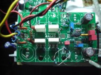
Shaan you mean like in this photo.
Attachments
Last edited:
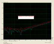
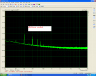
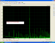
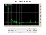
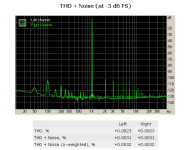
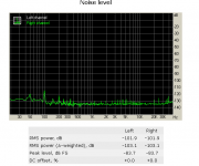
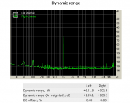
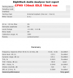
I haven't try the Shaan's last modification yet but i have modify the circuit(15K+4K7) for about 18mA VAS current and the idle current adjust to 136mA.
Here are the results.
Here are the results.
Attachments

c
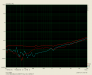
Using RMAA software.
Using RMAA software.
Attachments

Thimios - great job again! Good example, showing an importance of the layout nuances in overall build success - the devil is in the detail 🙂
Why is R17(R21) 10 Ohm added?
The resistors are for creating a CDRC filter in the PS rail to filter out more ripple before powering VAS/input. The diode is added to prevent VAS/input PS rail from sagging during loud transients.
Shaan, the amp schematics has gone through many iterations and some are representing proposals for improved modifications, it makes the discussion of the amp somewhat confusing, but lets straighten out a few things.
On a general note, when the audio signal enters the input stage it is ground referenced, but after T1(T2) there is a level shifting, the audio signal is not anymore ground referenced, this is very important to keep in mind, it is now split up and referenced to + and - rails respectively.
That means, when the audio signal enters the VAS stage T3(T4), these transistors must have both base and emitter referenced to the same + and - rails, but when adding a 10R and another big electrolyte on the other end of the 10R that splits up the reference point between base and emitter for these VAS transistors, they now have 2 different references with respect to the signal to work against, this is suboptimal, please remove R17(R21) and add a short in place of these resistors.
Last edited:
- Home
- Amplifiers
- Solid State
- CFH7 Amp