Modified Layout
Sorry if I forgot to mention a few collaborate on PCB.
Thiago
D1 and D2 will mitigate against the output stage diverting current away from the capacitance multiplier at high power levels.
The capacitors in the latter will not be affected due to the blocking effect of the diodes and since music is asymmetric it will be possible for the capacitance multipliers to recharge on opposite cycle swings.
I still think the supply rails would be cleaner if the source was a separate secondary set of bridge rectifier - remote as the main set.
This could still be a build option if D1 and D2 are removed to allow connection of this. You could make this an option by including pins on the open side of the thus "removable" diode connections. It is part of human nature to add one's personal touches to a given design.
At some stage you will need to build a prototype to evaluate the circuit and check the stability for your benefit and that of others. I think you could be doing this now.
As far as an output coil is concerned there is a question mark as to where to locate it since coils have fields around them. Distance from the main board solves that problem and if you do that you can experiment with the number of turns in the coil since you won't be needing to solder/de-solder your pcb.
On the 0R22 and 0R47 issue, wirewound resistors have a small amount of inductance which can be helpful in terms of stability. Probably 5 watt 0R47 have more than 2.5-3 watt 0R22. This might relax the amount of inductance needed for an output coil - with the Miller compensation method you will need to have one.
If you encounter problems with stability you could increase the value of the Miller capacitors but the difficulties continue there is another method you could try. The difficulty I see is the two feedback paths from the output are have low impedance and these connect to inverting inputs.
Miller capacitors can influence the forward transmission path but not the return path. The alternative compensation method is to get in ahead of the queue of the return signals on the other side of the feedback resistor.
Nice work Thiago. Have you run the Tina sim yet with this configuration? Please post Tina file if you can.
Thanks,
X
Thanks,
X
I'm back and having a quick look.
1. I suggest that the presets used to adjust offset are required only on one side. Keep R10 at a fixed value. R9 can be split into two resistors. One fixed at say half the value of R10 . The preset in series can be twice that value or equal to R10.That gives correction in both directions +/and -.
2. I think the clamping zeners are incorrectly placed. The two diodes are OK but the bottom zener is reversed . Also the junction of the zeners must join the output line.
3. The cap multiplier looks OK but the value of R25/R28 should be decided. I used 47K.Gives just over 1 volt as Vce for T10 and T11.
4. C17 and C20 probably don't need to be 100uF. It does not contribute to the filtering function of T10 and T11. Just a low impedance path to HF. Even a 10uF or lower should do....if required.
5. Be careful about the miller caps on the Vas. As it increases the slew rate falls , loop gain falls at HF and overall distortion goes up !
Last edited:
Nice work Thiago. Have you run the Tina sim yet with this configuration? Please post Tina file if you can.
Thanks,
X
Attachments
I'll pass on the simulations I use LT Spice and I have not been able to get it to convert.
Anyway re ashok's observation about cap values the large warehouse suppliers stock a range of manufacturers products so you can look at their product line up or research the low impedance types from manufacturers websites - the feedback loop in this is low impedance. For 63v types the lowest value stocked might be more than 10uF in that voltage range.
With regard to Miller capacitors you will have to do a frequency sweep simulation to study the gain and phase traces. As a rule the gain should reduce to unity at a point where the change in phase is 135 degrees or less.
With a FET output stage the changes in phase occur at much higher frequencies than with BJT version and there should be plenty of feedback for audio signals - so the value for the Miller capacitor doesn't need to be so great. You should have enough current from the input pair to allow some scope for increasing the capacitor values if the current is 3 m.a.
hi XRK971,
for 2nd GB of CFH9 please add me
- Iancortez 2 PCBs
- Jacques Antoine 2 PCBs
- Zman01 (TBC) 2 PCBs
- schillg11 2PCBs
Best regards
Günni
I think this is the latest GB list. I really like Thiago's but it is so different that we may run into a case of a board that needs debugging again. I would feel more comfortable with Marc's board, revised with suggestion based on actual tests and debugging by Thimios. Marc is still working on the revised layout once we have 6 interested people I will order GB2.
The trouble with instability is the feedback signals that can give rise to this lie above the audio spectrum.
The period of rise and fall times of a square wave equates to a higher frequency than that of the fundamental - the standard test being 10kHz into 8 ohms with a capacitor in parallel to induce a delayed feedback return signal into the output connection.
The test oscilloscope shots show some large spikes - overshoots on the leading and trailing edges of square wave into 8R//C can affect the character of the sound - if there is only one small overshoot it could pass as inaudible but not if it is a large of followed by a pattern of smaller ones - the result would be an edgy over-bright overtone.
It can be seen from the test shots how long it takes for irregularities to settle. Settling time is a parameter to be seen in IC op.amp spec sheets. With 8R//C loads an extreme value for C would be 2uF, however smaller values can upset some amplifiers through causing resonance at a higher frequency.
A lot of confidence has been placed in the results seen however this applies to only one built example and the work has not been finalised in laying out the board. The internal layout of the amplifier and other detail such as the routing of wire are other matters where variations could affect results.
FET output amplifiers obviate some shortcomings with BJT's but their extended frequency response needs to be managed - that implies using as many test as possible to exclude the possibility of hidden bugs.
Although it would be ideal if these were as good as each other - for the present who knows how good the alternative board layouts under review will turn out to be.
Last edited:

thiago,
The 10uf/63V and 22uf/63V elco parttern you use are not adapted as they are most 2.5 or 3.5mm pin spaced : exemple of 22uf/63 panasonic FC taht exist in 2.5 an 3.5mm pitch but no 5mm pitch. For 10mm it's worst as they exist in 2 or 2.5mm pitch.
Marc
The 10uf/63V and 22uf/63V elco parttern you use are not adapted as they are most 2.5 or 3.5mm pin spaced : exemple of 22uf/63 panasonic FC taht exist in 2.5 an 3.5mm pitch but no 5mm pitch. For 10mm it's worst as they exist in 2 or 2.5mm pitch.
Marc

Thanks
....
Thiago
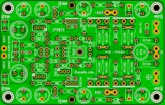
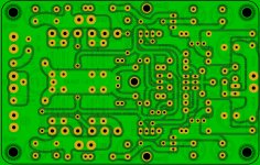
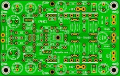
There seems to be parts everywhere surrounding the output mosfets so how do you mount them on heatsink?
Fab
There seems to be parts everywhere surrounding the output mosfets so how do you mount them on heatsink?
Fab
I do not think that would be a problem. Just leave a space.
Thiago
Attachments

It's a beautiful board. Very tempting to place order for PCBs now. We need more eyes to go over it though.
I do not think that would be a problem. Just leave a space.
Thiago
Indeed a space is required.... with also a small washer to attach firmly and uniformly the mosfets surface to heatsink..but still ok for diy since not à class A amp.
Fab
Last edited:
There seems to be parts everywhere surrounding the output mosfets so how do you mount them on heatsink?
Fab
Have a look at the picture in post 439 to see how this is practical.
In the last regard the leads to the FET's should not be made unduly long in the interests of avoiding oscillation - the gate pins should be as close to the device as possible to maximise the low pass these have in combination with the gate capacitance of the devices. It could be tricky to get that right - I see a 2u2 capacitor under a FET outline.
A second thought is it would make the job easier if that was less cramped for space.
A second thought is it would make the job easier if that was less cramped for space.
Thiago it looks great and I like also those curvy traces, but the Zobel network on the output... 
The RC should preferably be connected before the output inductor, also please add some space between the output transistor source resistors so they don't become too cozy with each other, it can lead to some accidents! 😛
The RC should preferably be connected before the output inductor, also please add some space between the output transistor source resistors so they don't become too cozy with each other, it can lead to some accidents! 😛
Last edited:
Thiago please add some space between the output transistor source resistors so they don't become too cozy with each other, it can lead to some accidents! 😛
I was a little uneasy about that - the spacing of the paired FET's is also very close on the board in post 439. It seems marginable and a bit more breathing space would give more peace of mind. I have seen instances of the zobel following the coil - the Leach Low TIM amplifiers for instance.
One of the problems of a system using dual nfb paths is where to derive the take-off points. Normally this would be further towards the output - I would settle for how it is - in the circumstances of FET outputs and layout difficulties with two paths, changing this could be less helpful.
- Home
- Amplifiers
- Solid State
- CFH7 Amp