???????? ?????, ????????? ???????? ? ???????, ?????????????
research output stages load resistance change from 2 to 8 ohms, and source impedance of 100 ohms to 10.1 kohms
best regards
Petr
research output stages load resistance change from 2 to 8 ohms, and source impedance of 100 ohms to 10.1 kohms
best regards
Petr
kgrlee, do you mean, that those techniques (simming thermal conductance & lag and/or matching Vbes) will allow THD staying stable enough even when the bias circuit decreases the quiescent current?
Because it will decrease it... regardless...
I've done some measurements on this and found that the bias varied only a few % under transient conditions. The long-term heating will decrease the Vbe required for a certain Ibias, but the bias current does NOT change - the bias circuit reduces the bias voltage to keep the bias curent constant.
For long-term heating of course the bias is pretty stable, given a competently designed bias spreader.
Those transient changes will not produce measurable or audible differences.
jan
Bias servo has to run in the same manner as DC servo - no trace from it in the audio signal.
Good point; that is certainly true in principle. But the numbers are different.
Jan
Great.... what are you going to use?
-RM
It's a sound-card based WinAudioMLS Pro EX from Germany.
(Manufacturer)
Pretty accurate tool, assuming a good card is used.
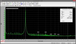
Just as an example of what it looks like, attached is 1kHz spectrum at 8 ohm resistive load, about 10V rms - my initial CFA prototype. Some 50Hz hum is visible (somewhere at -110db, but still).
Attachments
There are 2 quite separate issues.
Self devots nearly 1/5 of the 4th ed to Thermal compensation and thermal dynamics. Essential reading for those who want to work on this .. but I don't think his final solutions are correct.
- matching the Vbe multiplier to the output stage. Cordell is most detailed on this. It affects the bias when the amp has settled to whatever steady state signal. If you use the amp for sine waves this is sufficient.
- But if the signal changes, the thermal conditions also change and the bias must change with it. If the time constants aren't matched, you will have more distortion until the amp settles down to a new (hopefully) steady state. Where this hasn't been carefully thought out, the misbiased period can be 45s as Mr. Marsh to minutes as with Self
When the amplifier is switched on and begins to apply sinewave power to a load, the crossover spikes (generated by the deliberate underbiasing) will be seen to slowly shrink in height over a couple of minutes as the drivers warm up
Rather than pontificate on what I think is right, I offer my 1W THD test after high power as something all real PA designers should do.
______________
It may be that you like the slightly higher THD after a burst of high power with CFP. Or the higher THD at low level shown in Self's fig 5.39 & 5.40 4th ed that I posted slightly earlier.
Increased THD at low level, possibly due to xover, is known to be particularly audible to true golden pinnae in DBLTs.
Mr. Marsh, that's the bit I'm really interested to know if Self has done any new 'real life' work on in his 6th ed. I posted the pics in #5892. In the 4th ed, they are in Chapter 5 Output Stage I
You don't want the 'thermal loop faster'. You want it matched to the output stage/drivers etc. And the reason you want that is so its never improperly biased. And the reason you want that is for low THD cos xover is particularly nasty sounding.
kgrlee, thank you for lots of nuances
To put some numbers on it, this is a figure from my upcoming article in Linear Audio Vol 8.
You can see that at the end of a transient, Ibias recovers slowly.
Yet, look at the Ibias-variation on the right side axis - a few mA at best.
That means that a nominal Ibias of, say 60mA varies between say 58 and 62 mA. That will not be audible, and not be measureable.
Jan
You can see that at the end of a transient, Ibias recovers slowly.
Yet, look at the Ibias-variation on the right side axis - a few mA at best.
That means that a nominal Ibias of, say 60mA varies between say 58 and 62 mA. That will not be audible, and not be measureable.
Jan
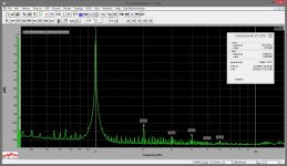
Attachments
It's a sound-card based WinAudioMLS Pro EX from Germany.
(Manufacturer)
Pretty accurate tool, assuming a good card is used.
Just as an example of what it looks like, attached is 1kHz spectrum at 8 ohm resistive load, about 10V rms - my initial CFA prototype. Some 50Hz hum is visible (somewhere at -110db, but still).
Did you try ARTA ARTA Software from Croatia.
What sound card are you using?
Did you try ARTA ARTA Software from Croatia.
What sound card are you using?
No, never heard about Arta... looks not bad at a first glance
I use E-MU 1616m pro-grade sound card (24/192 resolution).
(E-MU 1616m)
The major downside - 20kHz bandwidth. Looking if I can get something with wider bandwidth
You aren't heating the amp up sufficiently and long enough.You can see that at the end of a transient, Ibias recovers slowly.
Yet, look at the Ibias-variation on the right side axis - a few mA at best.
That means that a nominal Ibias of, say 60mA varies between say 58 and 62 mA. That will not be audible, and not be measureable.
Have a look at my previous post on how to test this. It's what happens when you have a soft passage after a long, very loud passage.
I suggest you measure THD instead of just looking at Ibias.
And try it on a CFP output stage.
What about Laterals, when they are biased near their neutral temperature point ?To put some numbers on it, this is a figure from my upcoming article in Linear Audio Vol 8.
I always try to be fair...but I prefer the relationships with gentlemen and sensible people.We have to be fair Esperado,
Does knowledge of music theory makes the talent of a musician ?
Last edited:
Question for you. Below I’ve got a very simple circuit so called CFA as a simple voltage follower removing all unnecessary complications. 450 Ohm feedback gives nice response. Now I make it 20k and gee wiz the BW is down over 10X and now I have to give a huge input step to make it slew. Wazzup, please explain this behavior without referring to the current in the feedback resistor because after all it can’t matter, the feedback is voltage. Actually caught MikeK on this, his knee jerk reaction was that the current in the feedback resistor did not charge the comp cap (he corrected himself but went on ignoring it).
Mr. Wurcer,
I have no idea of, and no interest in, you quarrel with MikeK. What you are showing here is a textbook example of the specific properties of a "CFA" (feedback network dependent open loop gain/ULGF, and feedback network dependent slew rate).
Not sure what made you believe that I share MikeK's opinions on the CFAs. My position is that what the industry calls (marketing driven, IMO) "CFA" is in fact a specific circuit topology (and AD844 is a good example), and is not, by any means, related to the feedback type. The feedback type is, for any purposes, still shunt (output) series (input) and can be analyzed using the canonical voltage feedback formalism. The fact that lowering the feedback resistor both increases the bandwidth, and as a result increases the small signal slew rate (or lowers the rise time, if you prefer), also increasing the current available to load the compensation capacitor (hence also increasing the large signal slew rate), is a specific property of this circuit topology. If you want to call this "current feedback" so be it, but please, again, don't tell me this is a new type of feedback, beyond the four well known types. Several hundred posts ago it was shown an example (LM6171) of a "current feedback" amplifier, without current on demand (that is, still has the open loop bandwidth modulated by the feedback network, but e.g. the current available to load the compensation cap is not) and several examples of (almost) classic VFAs having the current on demand property (and hence allowing slew rates of 300-500V/uS).
If there is any, my quarrel is with the CFA fan club, which absurdly insists that CFAs have some magic properties that contradict the very basic feedback theory (like allowing more loop gain to linearize, without degrading the stability margins, etc...) and that in particular for audio, where due to the rather large closed loop gains (>20dB) even the standard CFA specific properties are pretty much long gone.
I will go back to simply ignoring you.
That's fine, no problem, you already granted way to much attention to a poor student from across the pond.
Last edited:
My position is that what the industry calls (marketing driven, IMO) "CFA" is in fact a specific circuit topology (and AD844 is a good example), and is not, by any means, related to the feedback type.
Informing and helping customers get their job done is not marketing "hype". The application flexibility is not available in (some) other topologies without bringing out the frequency compensation nodes, at current amplifier bandwidths this is an applications nightmare. I don't see any pernicious motives in making and selling these amplifiers along with all the others. No one in the industry AFAIK has attributed any "magical" properties to any of these amplifiers, in fact the inferior DC issues like bias current, offset, and noise are well documented.
nice amps 🙂 but i wanted to share what i use to quickly check for oscillation lacking a scope; a probe, with a not too large coupling capacitor, with some high ohm resistor to ground, and a fast (germanium) diode to a DMM measuring DC. if it reads something it oscillates (or has some other signal on it).
I see the same thing happen with EF2 output..... after the signal is removed, the bias drops to very low level for awhile and then slowly returns to set level.
This is a bias circuit issue not an OPS issue/type. yes?
THx-RNMarsh
This is a good point, and true. Things heat up during high power, compensating the output stage, then when power goes very low, parts of the output stage cool down before the heat sink cools down. This is why ThermalTrak transistors are far superior. This is all discussed in my book.
Also, if you look at my old MOSFET power amp paper, you can see experiments of this phenomenon for both BJT and MOSFET output stages, showing this kind of transient thermal stability is far superior in MOSFETs.
In a Triple, a good solution is to have the pre-drivers and drivers are all mounted together on a common heat spreader/heat/sink, and that heat sink also has a temp sensor diode/transistor to do bias spreader compensation for those devices.
Cheers,
Bob
Bob Cordell,
I have been watching an learning from all this information about bias drift related to dynamic temperature changes and have a simple question. When looking at most circuits and the schematic layouts what I see often are the final output devices mounted on the edge of the pcb so that they can simply be mounted to the heat sinks, but the pre-driver and the driver transistors are often in the middle of the board away from and impossible to mount to the same heat sink as the power output devices. What is a good engineering solution to this problem, how can you mount these same devices on a common heat sink to solve the heat spread between the differing sections of the amplifier, and is the solution to the mounting of the pre-driver and driver transistors going to cause other problems that are just as important? In the layout of the design in the first place where optimization for lowest inductive currents and shortest path lengths are the driver of the circuit layout to begin with, are we just trading one set of problems for another?
I have been watching an learning from all this information about bias drift related to dynamic temperature changes and have a simple question. When looking at most circuits and the schematic layouts what I see often are the final output devices mounted on the edge of the pcb so that they can simply be mounted to the heat sinks, but the pre-driver and the driver transistors are often in the middle of the board away from and impossible to mount to the same heat sink as the power output devices. What is a good engineering solution to this problem, how can you mount these same devices on a common heat sink to solve the heat spread between the differing sections of the amplifier, and is the solution to the mounting of the pre-driver and driver transistors going to cause other problems that are just as important? In the layout of the design in the first place where optimization for lowest inductive currents and shortest path lengths are the driver of the circuit layout to begin with, are we just trading one set of problems for another?
No one in the industry AFAIK has attributed any "magical" properties to any of these amplifiers, in fact the inferior DC issues like bias current, offset, and noise are well documented.
I fully agree, you are talking about the industry professionals, I am talking about the diehard DIYAudio CFA fan club. Big difference, IMO, do I need to spell my opinion about the "high end audio" faith based culture?
Waly,
I don't think you are going to get much argument from many of us here about many of the claims that are made in the audiophile market. Yes there are those true believers who will take anything that some manufacturers says in their marketing literature as true statements but I bet the majority here don't fall into that category. It is a few and very verbal minority that keeps bringing up these magic powers and unmeasurable results over and over again. At the same time I think most of us recognize that the current test protocols are limited as to the correlation of say THD and final sonic qualities. There is something missing or inaccurate in how we are looking at some of these values.
I for one can't understand Fanboys and how they can drink the Koolaid, some companies can seem to do nothing wrong, they never actually look inside the item and check the build quality, some things would just be very obvious but they would deny these simple truths.
Bob Cordell,
I have been watching an learning from all this information about bias drift related to dynamic temperature changes and have a simple question. When looking at most circuits and the schematic layouts what I see often are the final output devices mounted on the edge of the pcb so that they can simply be mounted to the heat sinks, but the pre-driver and the driver transistors are often in the middle of the board away from and impossible to mount to the same heat sink as the power output devices. What is a good engineering solution to this problem, how can you mount these same devices on a common heat sink to solve the heat spread between the differing sections of the amplifier, and is the solution to the mounting of the pre-driver and driver transistors going to cause other problems that are just as important? In the layout of the design in the first place where optimization for lowest inductive currents and shortest path lengths are the driver of the circuit layout to begin with, are we just trading one set of problems for another?
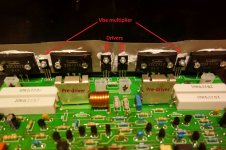
Just to share a practically refined, well-tested solution (which is pretty much in line with Bob Cordell's recommendation).
I mostly use EF3s in my designs. I put pre-drivers on the small individual aluminium heatsinks.
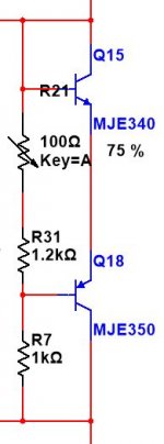
The drivers are at the common main heatsink with the output devices. 2 Vbe multiplier transistors are either between the big ones (if I use 2 pairs), or between the big ones and the drivers (if I use 1 pair).
Vbe multiplier - one of two transistors is used as a diode, in this case thermal feedback is just about right (otherwise, it slightly over-compensates).
This design is heavily tested in both VFA and CFA amplifiers, demonstrating good thermal stability.
Attachments
- Home
- Amplifiers
- Solid State
- CFA Topology Audio Amplifiers