Was told a long time ago that those type OPS transistors were not made any more. NOS somewhere or was I told wrong?
Rich,
NJL0281D (NPN) NJL0302D (PNP)
NJL3281D (NPN) NJL1302D (PNP)
are active products
ON Semiconductor
set filter TO-264-5 package
Kindhornman, having drivers on the same heatsink as the outputs is a problem. Parallel outputs close is good, drivers and outputs close is bad. Vbe drops as temeprature increases, so two diodes in series have twice the tempco, twice the problem - that's what a double EF is, two emitter junctions in series. That's why it's become popular to have the drivers some distance away on their own heatsink, like Vzaichenko and OS do.
Bob Cordell,
I have been watching an learning from all this information about bias drift related to dynamic temperature changes and have a simple question. When looking at most circuits and the schematic layouts what I see often are the final output devices mounted on the edge of the pcb so that they can simply be mounted to the heat sinks, but the pre-driver and the driver transistors are often in the middle of the board away from and impossible to mount to the same heat sink as the power output devices. What is a good engineering solution to this problem, how can you mount these same devices on a common heat sink to solve the heat spread between the differing sections of the amplifier, and is the solution to the mounting of the pre-driver and driver transistors going to cause other problems that are just as important? In the layout of the design in the first place where optimization for lowest inductive currents and shortest path lengths are the driver of the circuit layout to begin with, are we just trading one set of problems for another?
These are good points and questions. The first big decision is what if any of the pre-drivers or drivers to mount on the big heatsink along with the power transistors. If you mount only the power transistors on the big heatsink, then, as you mention, the pre-drivers and drivers will be back further on the board. Thermal stability wise, they are not as big a culprit as the output transistors, since they dissipate less and often operate in class A. But they will usually need a heat sink, at least for the drivers, if an adequate amount of current is flowed in the EF driver to sweep out the base of the output transistors at turn-off.
My preference is to mount the drivers and pre-drivers to a single heat spreader, often that may extend across the board. A simple strip of 1/16 aluminum by 1" tall will usually do. Often, no fins required. A separate Vbe multiplier for the pre-drivers and drivers (about 4Vbe for a Triple EF) is then used as part of the bias spreader. There will still be a Vbe multiplier for the output stage, and its transistor will typically be mounted on the big heat sink. I mentioned this approach in my book.
Another approach is to use the Diamond Buffer Triple (DBT), where the output transistor EF is preceded by a diamond buffer. If the pre-driver and driver on each side are mounted back-to-back on a common heatsink, good cancellation of the Vbe tempco of these devices will result.
Cheers,
Bob
Rich,
NJL0281D (NPN) NJL0302D (PNP)
NJL3281D (NPN) NJL1302D (PNP)
are active products
ON Semiconductor
set filter TO-264-5 package
Thx Dimitri -
I had met and talked to the inventor of the idea to put the bias diodes inside the power device package - the year they came out. Some time later on, i saw him at the same convention place and he told me they were not going to make them any more because of this and that reason... dont recall.... think it was a money decision only.
So, ON picked it up and is carrying the torch. I dont follow some of these things as closely as I ought to. But, life exists on other planets and I am going there next week... might have to be there for 3 months to get things done (and have fun, too). Hard to stay focused on audio electronics and keep up to date with so many distractions. 🙂
THx-RNMarsh
Bias ---- when the OP signal level is causing current draw from the OPS which is significantly higher than the set idle current ----- dropping the idle bias current/volts to zero during high levels of current draw has no affect on THD.
So, my conclusion is that the THD and idle set point are most important on how the first few watts are going to sound. Measurements at full power isnt so important as those at low levels. But the low level THD is, or can be, greatly affected by the high current via the thermal affects/bias changes.
THx-RNMarsh
Last edited:
If you are looking for a geometrical solution to mount drivers and power devices on the same heat sink, without sacrificing anything like shortest connections etc... just have a look to the brilliant VSSA's implementation ;-)how can you mount these same devices on a common heat sink to solve the heat spread between the differing sections of the amplifier, and is the solution to the mounting of the pre-driver and driver transistors going to cause other problems that are just as important? In the layout of the design in the first place where optimization for lowest inductive currents and shortest path lengths are the driver of the circuit layout to begin with, are we just trading one set of problems for another?
I fully agree, you are talking about the industry professionals, I am talking about the diehard DIYAudio CFA fan club. Big difference, IMO, do I need to spell my opinion about the "high end audio" faith based culture?
In that case I apologize for being a little overly energetic in my response. The topology is as old as the hills, I think some of the simplifications are harmless and help folks get where they want to go.
I think some of the simplifications are harmless and help folks get where they want to go.

-RM
Just to share a practically refined, well-tested solution (which is pretty much in line with Bob Cordell's recommendation).
I mostly use EF3s in my designs. I put pre-drivers on the small individual aluminium heatsinks.
The drivers are at the common main heatsink with the output devices. 2 Vbe multiplier transistors are either between the big ones (if I use 2 pairs), or between the big ones and the drivers (if I use 1 pair).
Vbe multiplier - one of two transistors is used as a diode, in this case thermal feedback is just about right (otherwise, it slightly over-compensates).
This design is heavily tested in both VFA and CFA amplifiers, demonstrating good thermal stability.
I did it a bit differently, pre-drivers are small and dissipate little and no heathsink, drivers and be multiplier transistor are on separate small heathsink, and only output transistors are on the main heathsink and off course TT diodes assisting Vbe multiplier.
Attachments
nice amps 🙂 but i wanted to share what i use to quickly check for oscillation lacking a scope; a probe, with a not too large coupling capacitor, with some high ohm resistor to ground, and a fast (germanium) diode to a DMM measuring DC. if it reads something it oscillates (or has some other signal on it).
😎 a nice little RF detector probe application.
You can also buy one from Ramsey Electronics - on ebay for $28.
-RM
Last edited:
I did it a bit differently, pre-drivers are small and dissipate little and no heathsink, drivers and be multiplier transistor are on separate small heathsink, and only output transistors are on the main heathsink and off course TT diodes assisting Vbe multiplier.
Nice implementation.
Cheers,
Bob
I did it a bit differently, pre-drivers are small and dissipate little and no heathsink, drivers and be multiplier transistor are on separate small heathsink, and only output transistors are on the main heathsink and off course TT diodes assisting Vbe multiplier.
A short side comment, I've noticed that most implementations here are placing the output inductor on the PCB. This is, in my opinion, a very bad idea. The magnetic field couplings (in particular at high output powers) are guaranteed to add a useless spread of even order harmonics. I would place the output inductor, and the parallel damping resistor, as close as possible to the speaker connectors, and as far as possible form any signal cables.
Good night.
😎🙂
Thanks everyone for the comments on the device mounting. I've been out building an engine so haven't seen the responses until now.
Christophe,
I have a pair of the VSSA boards from Lazy Cat. I look at how he laid that out.
Waly,
When you say to move the inductor off the board are you talking about putting the inductor immediately before the speaker leads or right at the speaker terminals? I guess you are just saying to keep them away from the rest of the power amp circuit and any traces or components.
Some thing i am not getting.. when you look at the On-semi application note for the Thermal Track, it seems like 3 pair of OPS devices require 6 diodes in the bias string.. would two devices then also require 6... ?? there must be an optimum number of diodes to get the OPS thermal tracking optimally. My gut feel says that two (and a resistor) should do it, How else could they make an amplifier with just one pair of output devices.??
A short side comment, I've noticed that most implementations here are placing the output inductor on the PCB. This is, in my opinion, a very bad idea. The magnetic field couplings (in particular at high output powers) are guaranteed to add a useless spread of even order harmonics. I would place the output inductor, and the parallel damping resistor, as close as possible to the speaker connectors, and as far as possible form any signal cables.
Good night.
Oh yes, I have read about that here many times but not supported with any measurement. D. Self does not say that in his book, just that is better to position it closer to the input then to the output devices(so it's on the PCB). Self writes about a crosstalk between two channels if the inductors are near and parallel.
Kindhornman, having drivers on the same heatsink as the outputs is a problem. Parallel outputs close is good, drivers and outputs close is bad. Vbe drops as temeprature increases, so two diodes in series have twice the tempco, twice the problem - that's what a double EF is, two emitter junctions in series. That's why it's become popular to have the drivers some distance away on their own heatsink, like Vzaichenko and OS do.
This is a very general a statement Keantoken.
Yes, separating OP devices from drivers/pre-drivers is one way as advocacy by Bob and Doug Self. But there other ways as well, like the two point method I used in my e-Amp.
I will write up my method as a separate article shortly.
Inductors can be mounted on the main PCB - just make set the orientation is good and well away from the IPS.
Fusible Resistor
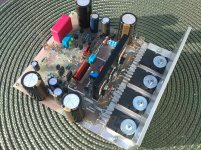
Hello Dadod,
I like your amplifier build, but I would like to say that it is good to use fusible or non flammable resistors on the output stage as it prevents board damage with an output stage failure . They look like carbon on the bases on the output devices I would use fusible types , I m not sure what RE (0.22R ) types you are using but I would use metal oxide types there if you are not already.
"I had met and talked to the inventor of the idea to put the bias diodes inside the power device package - the year they came out. Some time later on, i saw him at the same convention place and he told me they were not going to make them any more because of this and that reason... dont recall.... think it was a money decision only. "
Richard, it was in fact Barney Oliver that first proposed this in 1970 in his Class B crossover distortion paper.
🙂
Richard, it was in fact Barney Oliver that first proposed this in 1970 in his Class B crossover distortion paper.
🙂
Last edited:
- Home
- Amplifiers
- Solid State
- CFA Topology Audio Amplifiers