Dadod, Damir. What was your impression for the thermal compensation on your TMC amplifier, did it thermally fit with the 4 tracking diodes you were using.
I've experimenting with a sort of 3D-power amp module, with the aim to a) put everything in the output stage on the heatsink, and b) make all connections including to the power supply very short but still away from sensitive circuit parts.
One implementation shown in the pictures - you can see that the (pre) drivers are on the inside of the aluminum bars. The power supply connections are short and orthogonal to the board.
As Bob noted, putting (pre)drivers on the main heat sinks can be too much for thermal stability, so I now would do it different, placing the (pre)drivers on the PCB with their own small heatsink.
However such a module approach is very good electrically, with very little crosstalk and almost no supply induced distortion. Also for servicing you can just replace a complete module very easily and quickly.
Jan
Wow this looks great.
Where are you getting all the aluminum from? Do you by stock bars and mill them yourself?
It was perfectly appropriated, on my point on view. "he diehard DIYAudio CFA fan club." was just an insult for *all* the people interested in this thread and CFA's amps in general.being a little overly energetic in my response.
Dadod, Damir. What was your impression for the thermal compensation on your TMC amplifier, did it thermally fit with the 4 tracking diodes you were using.
I used the bias spreader suggested by B. Cordell in his book. It uses two TT diode in the bias spreader transistor emitter and has possibility to adjust the thermal compensation. With this bias spreader it's possible to use only one output TT transistor pair. You can find that in mine TT amp schematic.
Servicing is VERY easy - loose 4 bolts, disconnect wires and replace whole module.
Jan
When I said it's not easy serviceable I meant for us DIYers. We don't just change whole module, but try to replace the faulty component, and for that is better if you don't need to dismantle the hardware. Access from the PCB back said is important.
CFA because ---
See if you can find your copy of Electronics & Wireless World July 1987. An article by E.MARGAN is "Crossover distortion in Class B amplifiers.
View attachment WW Class B.pdf
"..... when the class B output generates distortion the voltage gain stage is having a hard job to rebalance the error sensed by feedback, but it can only react with its own open-loop bandwidth and gain. ....... the distortion generated with class NSB operation is very close to the noise floor. These figures are the same as can be achieved with class A."
* NSB = No Switching B
THx-RNMarsh
I used the bias spreader suggested by B. Cordell in his book. It uses two TT diode in the bias spreader transistor emitter and has possibility to adjust the thermal compensation. With this bias spreader it's possible to use only one output TT transistor pair. You can find that in mine TT amp schematic.
See if you can find your copy of Electronics & Wireless World July 1987. An article by E.MARGAN is "Crossover distortion in Class B amplifiers.
View attachment WW Class B.pdf
"..... when the class B output generates distortion the voltage gain stage is having a hard job to rebalance the error sensed by feedback, but it can only react with its own open-loop bandwidth and gain. ....... the distortion generated with class NSB operation is very close to the noise floor. These figures are the same as can be achieved with class A."
* NSB = No Switching B
THx-RNMarsh
Last edited:
Wow this looks great.
Where are you getting all the aluminum from? Do you by stock bars and mill them yourself?
No I don't have milling capability. I design around stock material of the hardware store 😉
I do my own cutting, drilling and tapping of course, and I have a place here that does powder coating of 'prototypes' for a reasonable price.
Jan
No I don't have milling capability. I design around stock material of the hardware store 😉
I do my own cutting, drilling and tapping of course, and I have a place here that does powder coating of 'prototypes' for a reasonable price.
Jan
You have a better hardware store than I have.
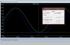
This is the distortion (20 KHz/80V/p-p on my Non switching error correction OPS running open loop with a gain of 1.
A non global feedback amplifier is in the making.
Harmonic Frequency Fourier Normalized Phase Normalized
Number [Hz] Component Component [degree] Phase [deg]
1 2.000e+04 4.023e+01 1.000e+00 -0.46° 0.00°
2 4.000e+04 1.033e-03 2.568e-05 12.41° 12.87°
3 6.000e+04 5.992e-04 1.489e-05 -85.51° -85.05°
4 8.000e+04 9.264e-06 2.303e-07 -94.70° -94.24°
5 1.000e+05 2.299e-04 5.714e-06 89.82° 90.27°
6 1.200e+05 3.884e-05 9.654e-07 15.11° 15.57°
7 1.400e+05 7.236e-05 1.799e-06 102.73° 103.19°
8 1.600e+05 1.987e-06 4.938e-08 -3.26° -2.81°
9 1.800e+05 4.298e-05 1.068e-06 110.33° 110.79°
Total Harmonic Distortion: 0.003032%
This is the distortion (20 KHz/80V/p-p on my Non switching error correction OPS running open loop with a gain of 1.
A non global feedback amplifier is in the making.
Total Harmonic Distortion: 0.003032%
In combination with the GainWire as the gain block could be good amp. Could you show the schematic?
Damir
Sorry Damir for various reasons I can't disclose the OPS. I am only one of the parties that has been developing the circuit.
Hello Dadod,
I like your amplifier build, but I would like to say that it is good to use fusible or non flammable resistors on the output stage as it prevents board damage with an output stage failure . They look like carbon on the bases on the output devices I would use fusible types , I m not sure what RE (0.22R ) types you are using but I would use metal oxide types there if you are not already.
hello,
there can be a couple of problems with fusible resistors.
1-they can be nonlinear near the fuse point.
2-Because each transistor is now fused when one blows it severely throws off the balance of the remaining transistors
A short side comment, I've noticed that most implementations here are placing the output inductor on the PCB. This is, in my opinion, a very bad idea. The magnetic field couplings (in particular at high output powers) are guaranteed to add a useless spread of even order harmonics. I would place the output inductor, and the parallel damping resistor, as close as possible to the speaker connectors, and as far as possible form any signal cables.
Good night.
Hello,
it is important to remember that the inductors need to be oriented at 90° to each other, ideally aligned to the center of the device to minimize crosstalk.
Hello,
it is important to remember that the inductors need to be oriented at 90° to each other, ideally aligned to the center of the device to minimize crosstalk.
Such as ---

RM
Ahhh... my favorite Sankens 😛
Richard, what amp is it? Some commercial product...
Inductors are placed the right way
3D-power amp module

Cheers, E.
Very nice Jan!I've experimenting with a sort of 3D-power amp module, with the aim to a) put everything in the output stage on the heatsink, and b) make all connections including to the power supply very short but still away from sensitive circuit parts.
[snip]
Jan
Cheers, E.
😕 My pub (Hoppe, 020-NL) is still open. 😉Edmond! What happened - they closed your pub?? 😉
Jan
So, what do you mean?
Cheers, E.
- Home
- Amplifiers
- Solid State
- CFA Topology Audio Amplifiers