Why do I get the feeling that the "violin" Waly used means that he isn't surprised at the results he got. I would be happy with that sort of measured THD at that power especially for a prototype setup. It's a real life measurement and not spice.
One of the lessons I have learned from building the prototype is that topology/loop gain should not be the first on the list of priorities for an ultra low distortion amplifier. At 800W/40hm @ 1KHz where the distortions are about 0.002%, I can add or subtract the effect of 20dB of loop gain by moving the power supply and speaker wires around, not to mention changing the grounding layout.
20 amps of harmonic (load) and non harmonic (+/-power supplies) currents (as in any class AB amplifier) are difficult to fight with. Ultimately, braiding the supply lines, keeping supply and load wiring as much as possible apart, futzing with board positioning in the output stage proximity, changing the grounding layout, etc... did the trick, but I am still not sure that I measured only the intrinsic amp distortions or some mix with the D. Self's magnetic induced distortions.
I would expect that, in a finished amp (which I have no plan to pursue), wiring and the case layout would affect the final result much more than any ultra low distortion clever topology.
Last edited:
As usual, you did not answer any of my legitimate questions.
I wont even bother with the first half.
Please don't. You are only helping me to make my point.
One of the lessons I have learned from building the prototype is that topology/loop gain should not be the first on the list of priorities for an ultra low distortion amplifier.
I would expect that, in a finished amp (which I have no plan to pursue), wiring and the case layout would affect the final result much more than any ultra low distortion clever topology.
Hi Waly,
This is most others conclusions as well and for same reasons and has been pointed out by others along the way. The goal here was never to just make an amp of low distortion.... there are many approaches for that goal. Rather, to make a CFA topology amp that is as good as possible. We know VFA can be super good, but could CFA? Now we know thru various person's SIM work here that it can be every bit as good in the THD department.
THx-RNMarsh
Last edited:
One thing I agree, 800W/4ohm is not required in a home, even if one considers the speaker impedance dip, and the phase shift.
Well, depending on bias setting you will get up to 25 Watt/ch in class A. I think it was John Curl who wanted even more class A power from his designs.
No, it is not. The inverting input node impedance is Rfeedback/2. If the jfet would be replaced by a bipolar (with appropriate changes to the biasing), then the impedance would be approximately Rfeedback/2 || R1/4 which is lower, but not necessary hugely lower.
But the CFA aspect is given by the fact that the open loop gain depends on the feedback network, here OLG~[250ohm/(R1/4+Rfeedback || 500ohm)]/[(Rfeedback+500ohm)/50ohm]. Something that never happens in a VFA.
You really need to learn how to break a feedback network and calculate the feedback network loadings. The equivalent schematic is attached.
FYI -- I published the complimentary push-pull version of this 35 years ago. And, it did much better than -100dB then.
What's new? .... other than scaled up to 800W.
THx-RNMarsh
Last edited:
One of the lessons I have learned from building the prototype is that topology/loop gain should not be the first on the list of priorities for an ultra low distortion amplifier. At 800W/40hm @ 1KHz where the distortions are about 0.002%, I can add or subtract the effect of 20dB of loop gain by moving the power supply and speaker wires around, not to mention changing the grounding layout.
20 amps of harmonic (load) and non harmonic (+/-power supplies) currents (as in any class AB amplifier) are difficult to fight with. Ultimately, braiding the supply lines, keeping supply and load wiring as much as possible apart, futzing with board positioning in the output stage proximity, changing the grounding layout, etc... did the trick, but I am still not sure that I measured only the intrinsic amp distortions or some mix with the D. Self's magnetic induced distortions.
I would expect that, in a finished amp (which I have no plan to pursue), wiring and the case layout would affect the final result much more than any ultra low distortion clever topology.
Interesting observations. Have to agree on layout being very important. In my prototype I can turn it into an oscillating mess by just messing with the grounding scheme. Likewise, just moving the power supply wires can observe changes in noise pick up.
IMHO, Loop gain, topology etc. sets the top end of what you can achieve and as such are important. But at the design stage it seems sensible to consider how you are going to implement it. For example, if you can reduce the number of ground connections in a design it may make PCB layout easier.
Magnetic distortions are an issue but if you can keep loop areas as small as possible then you can minimise both the "transmitters" and "receivers". The Cherry (I think it was Cherry) recommendation of running the power rails down the centre of the PCB is a good start. That reduces the worst loop to a minimum.
Your measurements are most likely a mix. You have implied this by stating that moving things around had 20dB affect.
Have you considered putting a Hawksford Error Corrected Output stage on your amp? With the ULGF you have it is a possibility.
yes. agree. noise. used in several places, commercially.... such as mixing consoles.
would be interesting in a powr amp app. usually more effective in reducing noise in higher gain areas, though.
-rm
It is a good thing that CFA allows for FB ratio change, without affecting stability that much. So we may get better S/N than in case of input pot + always maximum gain. I know you have understood what I meant, but probably not everyone did.
Of course, I would design them out when possible. With a line stage (low gain) circuits it is possible to not use them and still be direct coupled. With high gain, it is really hard. With power amps and their large thermal change potential it is a mixed bag - they are not high gain circuits but the temp can vary a lot without very large heat sinks.
I dont think it matters a lot when the servo only sees dc drift/offset. But generally, PP are not expensive, easy to find and work very well. It is more important in a servo to get the CMR and DMR dealt with in a 2 stage servo, perhaps. As John Curl has pointed out to me, recently.
Thx-RNMarsh
I have always used 2 stage dc servos. The single op-amp non-inverting servo is a serious compromise that only makes sense if dual op amps are expensive. The dual only needs one capacitor anyway. Use a PP cap between 0.1uF and 1uF and you are good. All explained in chapter 8 on servos in my book. The two-stage literally takes up less board space.
Going without a servo entails a worse capacitor choice unless you can go fully dc coupled.
Cheers,
Bob
It is not that you are wrong.... rather you missed the importance of the details I mentioned. Such as thickness. If the pcb copper (or plating) is thick 'enough' you wont see the effect. [Though you would if the power levels were increased and moved to higher freq. I discussed this with HP to make a more powerful addition to the test instrument and they were interested and gave some insider support info to me but we never did it]
Rough surface and edges are also a part of the known effects on UHF and contributes to impulse or rise time smearing/group delay. So, yes at high enough freqs this must be improved as well. Note that the effect I am measuring was not at those freqs ---> 100Hz to 100KHz. Where the effect is much weaker and/or can be dominated by other parameters.
The plating on parts or as a conductor - for audio - needs to be at least 1-2mil for audio so that the copper is thick enough to minimize the edge effect. In mass produced audio it is well under 1mil. And, SOTA attempts by DIYers need to be aware of this, IMO. But not if they 'like' distortion etc.... this info isnt for them.
Thx-RNMarsh
Richard,
You stated that the HF signal travels only on the edges of a trace. I disagree. That is all I was pointing out. In that regard, I don't think I missed any details. Do you still maintain that HF travels primarily on the edge of a trace, as you stated?
Cheers,
Bob
FYI -- I published the complimentary push-pull version of this 35 years ago. And, it did much better than -100dB then. What's new? .... other than scaled up to 800W.
Not sure what you are talking here about. JC's topology is not even remotely to what I have built.
I was only trying to show that while this topology has all the attributes and properties of a CFA, Mr. Curl itself calls it a VFA. That is in fact correct, because for the range of closed loop gains used in audio, the CFA specifics are long gone.
more details -
But not sure what you mean by Only. Yes... there is that tendency IF the trace is as I described ..... wide and very thin. That is what I was also told by physicist researcher doing high current pulsed power experiments. His transmission line (wide and thin... about 2-3 feet wide and inch thick aluminum) - said he found this was the case and it was causing him some issues.... called me over to see if I had any ideas about it and what he was trying to do... I have no reason to not believe him. It wasnt theoritical research but applied and he had an experiemnt that he was measuring. I was curious to see if it was true at lower freqs and currents and did the experiment I showed which seems to back him up.
Regarding the edge/surface smoothness. It is important when you want to keep waveform fidelity and especially for the leading edge. There are many parameters affected (reflections is another) and depends on which par is important to your system.... but this also means the path is longer.... a straight edge being shortest. The goal being minimized group delay and max waveform fidelity - no time smearing. In my researchers case he needed maximum peak energy in shortest time.
In your low current RF app, signal traces are not this shape.... more square and very small size where there would be nil such affect.... more evenly distributed.
The pcb trace I used would be Not unlike that found in high current areas of a power amp circuitry.
THx-RNMarsh
Richard,
You stated that the HF signal travels only on the edges of a trace. I disagree. That is all I was pointing out. In that regard, I don't think I missed any details. Do you still maintain that HF travels primarily on the edge of a trace, as you stated?
Cheers,
Bob
But not sure what you mean by Only. Yes... there is that tendency IF the trace is as I described ..... wide and very thin. That is what I was also told by physicist researcher doing high current pulsed power experiments. His transmission line (wide and thin... about 2-3 feet wide and inch thick aluminum) - said he found this was the case and it was causing him some issues.... called me over to see if I had any ideas about it and what he was trying to do... I have no reason to not believe him. It wasnt theoritical research but applied and he had an experiemnt that he was measuring. I was curious to see if it was true at lower freqs and currents and did the experiment I showed which seems to back him up.
Regarding the edge/surface smoothness. It is important when you want to keep waveform fidelity and especially for the leading edge. There are many parameters affected (reflections is another) and depends on which par is important to your system.... but this also means the path is longer.... a straight edge being shortest. The goal being minimized group delay and max waveform fidelity - no time smearing. In my researchers case he needed maximum peak energy in shortest time.
In your low current RF app, signal traces are not this shape.... more square and very small size where there would be nil such affect.... more evenly distributed.
The pcb trace I used would be Not unlike that found in high current areas of a power amp circuitry.
THx-RNMarsh
Last edited:
Is it possible to have an amp where the gain is variable by placing a pot in the feedback shunt position, and being stable with good step response across the gain range? And not just stable, but relatively consistent step response and phase margin? I think this should be possible for both VFA's and CFA's.
BTW, why would anyone call it a CFA and risk all that drama on the name? Why not just call it emitter-feedback or source-feedback? I see far less potential contention in that.
We used CFA-based equalizers back in 1971 on the Picturephone project at Bell Labs for this very reason. The equalizers were used in the analog repeaters spaced 1 mile apart. Combinations of these stages needed to equalize 22 AWG copper pairs out to 1MHz to better than a dB. To first order, the EQ shape was a square root of f response, as expected. Paralleled series R-C sections were placed in shunt in the emitter circuits to achieve the desired EQ curve. Frequency response of the equalizers was measured with a Computer Operated Transmission Measuring Set (COTMS) run by a PDP9. The filter systhesis program ran on an IBM370. The CFA topology was good for this example of variable gain as a function of frequency without painful interactions with the feedback compensation.
Cheers,
Bob
But not sure what you mean by Only. Yes... there is that tendency IF the trace is as I described ..... wide and very thin. That is what I was also told by physicist researcher doing high current pulsed power experiments. His transmission line (wide and thin... about 2-3 feet wide and inch thick aluminum) - said he found this was the case and it was causing him some issues.... called me over to see if I had any ideas about it and what he was trying to do... I have no reason to not believe him. It wasnt theoritical research but applied and he had an experiemnt that he was measuring. I was curious to see if it was true at lower freqs and currents and did the experiemnt I showed which seems to back him up.
In your low current RF app, signal traces are not this shape.... more square and very small size where there would be nil such affect.... more evenly distributed.
THx-RNMarsh
We must be having a semantics problem here. The traces I use, and just about everybody else uses on PCB are way not square in cross section. Even a 4-mil trace is far wider than it is high. Sounds like where you got your impression of HF traveling on edges was from an experiment that had little to do with the realities of the PCB traces we all use.
Cheers,
Bob
I was only trying to show that while this topology has all the attributes and properties of a CFA,
It has not. -IN input impedance, without global NFB applied, is high. In CFA, -IN input impedance is low even without feedback.
We must be having a semantics problem here. The traces I use, and just about everybody else uses on PCB are way not square in cross section. Even a 4-mil trace is far wider than it is high. Sounds like where you got your impression of HF traveling on edges was from an experiment that had little to do with the realities of the PCB traces we all use.
Cheers,
Bob
Semantics perhaps. More square than my example/test ratio. But maybe not? More Sq or not.... that wasnt the point --- Test was to see if only the HF could be affected by changing the path length at only the edge and noting the HF phase change and delay change compared to not modified.... at freqs within the BP of high performance amplifiers. The HF response was in fact affected by the increase at the edge. The size of the trace was based on application's current draw thru the pcb trace. High current traces in power amps would not be much different.
edge and surface variations are the same thing as far as results are concerned. A straight edge is the shortest path. The edge/surface irregularities lengthen the time at higher freqs... leading to waveform distortion. A number of other parameters can be measured... reflections being one.
We can go on expanding and explaining. Lets not do a tomb on this as the In's and out's are well doc else where.
THx-RNMarsh
Last edited:
It has not. -IN input impedance, without global NFB applied, is high. In CFA, -IN input impedance is low even without feedback.
No it is not. You can't consider in JCs topology Rfeedback only as part of the feedback network, it's part of the open loop gain as well. Hence, being always there, it also determines the inverting input impedance.
Anyway, you are not going to tell me that if the jfet would be replaced by a bipolar, that would change from VFA (high inverting input impedance) to CFA (low inverting input impedance), isn't it?
Last edited:
No it is not. You can't consider in JCs topology Rfeedback only as part of the feedback network, it's part of the open loop gain as well.
What do you call JCs topology, then? Halo JC-1 or anything else? Halo JC-1 is a VFA undoubtedly.
What do you call JCs topology, then? Halo JC-1 or anything else? Halo JC-1 is a VFA undoubtedly.
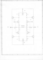
The attached schematic, that I already linked to, and that was posted by Mr. Curl in his thread.
Attachments
- Home
- Amplifiers
- Solid State
- CFA Topology Audio Amplifiers