170 mA is a bit too much. In my build IRFP OPS's bias trimmer is close to the edge, but I manage to set 80-90mA. If you put R21, R24 = 200-220R instead of 150R, you will lower the VAS current to appropriate level.
Those spikes on the curve look like the local OPS oscillation to me. Do you use 33pF caps at the drivers (base-to-collector)?
Interesting, what the difference is - my curves are crystal clear.
Those spikes on the curve look like the local OPS oscillation to me. Do you use 33pF caps at the drivers (base-to-collector)?
Interesting, what the difference is - my curves are crystal clear.
Hi Valery,
I think you are right. I just hooked the CF-FET up to the Tubsumo OPS and it looks perfect. I guess there is something not quite right about my IRFP OPS. I do have the 33p's installed. I would try it on my BJT OPS but I'm sure the output is too high.
I'd like to get to the bottom of the issue with the IRFP OPS. I have noticed a little spike on other IPS as well but not as pronounced. I hurt this OSP once by inadvertently hooking the rails up backwards. I had to replace all the diodes and a couple caps. I wonder if the 33p caps could have been hurt. I'll replace those and see if that changes anythng,
Thanks for your help.
Blessings, Terry
Guys, what is the advantage of this cascade connection? From my perspective, any wire, rather connector is a potential source of problems ... Can you explain why is the amplifier divided?
Guys, what is the advantage of this cascade connection? From my perspective, any wire, rather connector is a potential source of problems ... Can you explain why is the amplifier divided?
Hi Maxwell,
The concept of separate front-end / OPS modules was successfully used by the member Ostripper within his Slewmaster series of designs. In my designs, I use both single PCB (mostly for rather compact amps) and modular arrangements. Modules give a lot of flexibility, especially in DIY environment. You can test different conbination of IPS/OPS modules.
If you use the good plugs and arrange the wiring the right way - no problem at all. Even working with the bandwidth close to 1MHz. If decently arranged wiring between the modules causes stability issues - most likely there is a problem with the design somewhere.
In my current build, I have the front-end modules shielded and placed with their inputs close to the input plugs (external connections on the back panel), away from the heatsinks. At the same time, long 5-pair OPS modules are placed on the heatsinks, with the outputs close the output plugs. Performs wery well.
Cheers,
Valery
Hi Valery,
OK, I'll try this concept .. BTW Is it possible to buy PCB ? I think I am not able to do SMD PCB by my self 🙂
Regards,
Marcel
OK, I'll try this concept .. BTW Is it possible to buy PCB ? I think I am not able to do SMD PCB by my self 🙂
Regards,
Marcel
Hi Valery,
OK, I'll try this concept .. BTW Is it possible to buy PCB ? I think I am not able to do SMD PCB by my self 🙂
Regards,
Marcel
Hi Marcel,
Sorry - missed your post somehow. I am thinking about producing some boards - need to clarify a few things, will let you know if you are still interested 😉
Cheers,
Valery

Valery,
after following Pete's Slewmaster thread you don't think there will be any problems with the close spacing of the output devices? Will this limit the actual upper output levels or is that not as big a problem as OS found before he spread the outputs across his much longer output boards? I've been following your work since seeing your posts on the Slewmaster thread.
after following Pete's Slewmaster thread you don't think there will be any problems with the close spacing of the output devices? Will this limit the actual upper output levels or is that not as big a problem as OS found before he spread the outputs across his much longer output boards? I've been following your work since seeing your posts on the Slewmaster thread.
Very nice! I see you are using the vfet ops. Going to be a powerhouse.
Yes - good for driving some "difficult" speakers, having their impedance going down below 4 ohm at some frequencies 😎
Valery,
after following Pete's Slewmaster thread you don't think there will be any problems with the close spacing of the output devices? Will this limit the actual upper output levels or is that not as big a problem as OS found before he spread the outputs across his much longer output boards? I've been following your work since seeing your posts on the Slewmaster thread.
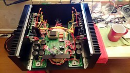
Hi Kindhornman - you're absolutely right, this arrangement is not optimal because of two reasons:
1) Output devices are too close;
2) Output devices' distribution is not symmetric across the heatsink.
As a result, not all the power potential of the housing is used.
I use +/-50V regulated rails for the front-end here, so some 140W @ 8 ohm is something I expect as a maximum power here.
I will definitely take these "flaws" in account for the next build 😉
Hi Valery,
What i find "too bad" on your build over the distance between output transistors, is that you just use the half capacity heatsink of your Amp case. All Power Mosfet are on one of the two heatsink constituing one side of the case. May be you could use a 10mm aluminium plate that spread heat over the two heatsink.
Marc
Exactly - this is what I mean by "not symmetric distribution". Well, enough for the purpose now, but for the next build I will place the output devices in a better way.
One more thing - it would be a good idea to place the speaker protection relays (mechanical or solid state) close to the output terminals. My OPS boards' output is very close to the terminals, but I have to use the long wires to connect both the OPS outputs and the terminals to the control board relays.
I can send you files for remote speaker relays. They will need to be altered to fit your binding posts though.
I can send you files for remote speaker relays. They will need to be altered to fit your binding posts though.
That would be cool - I will implement them here over the time then 😎
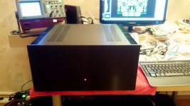
My lovely amp
Even with those "inefficiencies", just discussed above, it's a lovely amp 😎
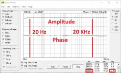
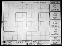
Did more accurate measurements - just a few pictures. Bode plot - only 2.4 degrees phase shift at 20 KHz - and 20 KHz square wave response - roughly 20V in 400 nS (RF filter is in place).
ONE PRECAUTION to the builders - in general, not only for this particular high-speed design - especially, dealing with the MOSFETs of any kind:
*** Clean your boards from the flux as much as possible ***
Make sure, they are clean and dry before switching on the power section. Many fluxes conduct pretty well. Not too much of a problem in relatively low-impedance BJT circuits, but a big problem in high-impedance MOSFET designs. Flux pulls the gate up (or down) to the rail, resulting in much higher quiescent current, than you would expect - and it can be significantly different between the push-pull pairs because of those flux spots here and there 😱
Even with those "inefficiencies", just discussed above, it's a lovely amp 😎
Did more accurate measurements - just a few pictures. Bode plot - only 2.4 degrees phase shift at 20 KHz - and 20 KHz square wave response - roughly 20V in 400 nS (RF filter is in place).
ONE PRECAUTION to the builders - in general, not only for this particular high-speed design - especially, dealing with the MOSFETs of any kind:
*** Clean your boards from the flux as much as possible ***
Make sure, they are clean and dry before switching on the power section. Many fluxes conduct pretty well. Not too much of a problem in relatively low-impedance BJT circuits, but a big problem in high-impedance MOSFET designs. Flux pulls the gate up (or down) to the rail, resulting in much higher quiescent current, than you would expect - and it can be significantly different between the push-pull pairs because of those flux spots here and there 😱
Attachments
Both channels are fully operational now 😎
Have to mount the front panel with the status LED and perform the listening tests 🙄
beautiful!
Finished!
Thank you Damir 😀
Here is the "final touch" 😉
It happens not too often, when I end up with completely built "product" - very happy I have finally finished this one 😛
beautiful!
Thank you Damir 😀
Here is the "final touch" 😉
It happens not too often, when I end up with completely built "product" - very happy I have finally finished this one 😛
Attachments
- Status
- Not open for further replies.
- Home
- Amplifiers
- Solid State
- CF-FET V2.0 front-end - going high-tech (SMD)