So it ran - however the BJT has a thermal runaway with the heatsinks being toasty.
screenshot-2022-07-03-at-11-30-34-png.1068979
Result is that I think the LED in one of the HV supplies (let's call that side "A" which is the left) started to toast but the 10R didn't nor did the others. So naturally I thought there must be a short in the BJT. The tube is fine and has been running at 9mA idle. 55R load resistor is fine but that's 5W.
It looks like the BJT is reading 0R between collector and emitter vs the other BJT that reads about 65R.
Looks like both NPNs are toasted 😀 The upper is 0R between all the pins and the bottom is not much better. I bought additional BJTs and mosfets for this reason.
I stand corrected the LED is fine (cut the BJT pins and powered up). I did a calculation it's 30mA max would have required 500V which would have blown the 350V caps. I noted something sparked but unsure what that was or was my imagination. All the power supplies have a big MURS diode across them to prevent voltages from reversing should they power down at different rates.
Now it would be dumb not to learn from the experience. Looking at the data sheet I think the 68R is using the bias too hard (44 or 50R may be better) but also there's a few options for temperature compensation using feedback and dropping the bias based on the current increase. The DC feedback should, in theory, manage a DC offset by chancing the tube bias - that would essentially feedback the NPN bias in the event that heat was increasing current. A better bet may be adding a bias temperature compensation based on the current.
On starting the amp I did note that both sides were sitting at -31Vdc on each side of the the 55R Load. A very different position for the modelled amp and without the BJT and LV power installed. I think the next step is to look at this - no BJT but run with the LV supply in place. I've been very careful with the AC and rectification to ensure all the supplies share the same phasing so any residual ripple is common.
The two sides are floating hence they will find their own equilibrium with the ground points being 1K away from the earth point.
i’ll investigate later.
So I've left the BJTs out of the equation and started to focus on simply the valve and the power supplies. The LV supplies don't have the 1uF caps nor the 220nF X cap on the rectifier side plus the entire amp doesn't have snubbers - hence the noise spread from the AC diodes:

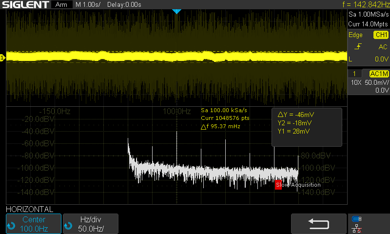
So the new AC top enclosure has helped reduce the noise. The remaining noise should be hit by the snubbers etc. I'm still getting a 40dB 100Hz mains noise:
Measuring the voltages without the BJTs in place shows the almost the same voltages seen when the BLTs are operational:
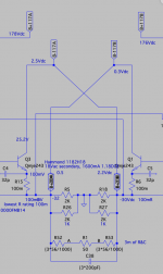
The tubes are sitting at -5.5V grid bias and about 10mA which is fine however the mosfets don't seem to be doing much but the voltages are all sat floating around the -24 to -30Vdc mark (at the Load), That differs completely to LTSpice. The only thing I think could happen is that the pads I'm using for BJT thermal connection to the heatsinks is grounding the amp some how causing the negative offset. Let me cut the remaining collector pins (which the back of the NPN is a collector pin 4).
Removing the BJTs from the grounded heatsink the FFT changes to this:
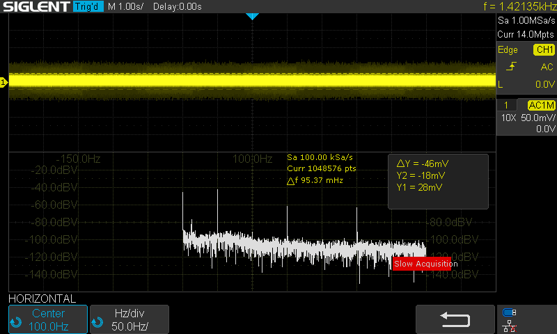
Note the missing 100Hz noise.. Holmes Interesting Dr Watson
Also the offset the LV power supplies are now sat at 0V ref with a 32.5V positive (not surprising as the BJT is hanging in the air without any over connections to the positive except the HV negative. the HV is now sat at 200V (ie HV+LV) with the tubes idling at 10mA. The 55R load is now sees 0V on either side.
So the BJTs were grounding (at least enough to cause a 2V drop) which drew enough to re-reference the entire load to -32Vdc! I'd removed the BJTs by cutting and separating the emitter and base pins leaving the collector connected to the LV power positive. That means the only physical connections were the collector and the back of the BJT which is a collector pad.
So that's was fun - it may also indicate why I had a runaway. I need new non- electrically conductive thermal pads. I used a similar series of pads with the MF A220 but the BUZ package is plastic and the pads are meant to be non-electrically conductive unless they break down when cooked or have some microscopic metallic particles puncturing the pad.
The amp now seems to be behaving like the LTSpice model. I was touching the heatsink and chasing over the time and didn't feel a thing (30V would have been felt) so that care doing the grounding was working nicely.
So the new AC top enclosure has helped reduce the noise. The remaining noise should be hit by the snubbers etc. I'm still getting a 40dB 100Hz mains noise:
Measuring the voltages without the BJTs in place shows the almost the same voltages seen when the BLTs are operational:

The tubes are sitting at -5.5V grid bias and about 10mA which is fine however the mosfets don't seem to be doing much but the voltages are all sat floating around the -24 to -30Vdc mark (at the Load), That differs completely to LTSpice. The only thing I think could happen is that the pads I'm using for BJT thermal connection to the heatsinks is grounding the amp some how causing the negative offset. Let me cut the remaining collector pins (which the back of the NPN is a collector pin 4).
Removing the BJTs from the grounded heatsink the FFT changes to this:
Note the missing 100Hz noise.. Holmes Interesting Dr Watson
Also the offset the LV power supplies are now sat at 0V ref with a 32.5V positive (not surprising as the BJT is hanging in the air without any over connections to the positive except the HV negative. the HV is now sat at 200V (ie HV+LV) with the tubes idling at 10mA. The 55R load is now sees 0V on either side.
So the BJTs were grounding (at least enough to cause a 2V drop) which drew enough to re-reference the entire load to -32Vdc! I'd removed the BJTs by cutting and separating the emitter and base pins leaving the collector connected to the LV power positive. That means the only physical connections were the collector and the back of the BJT which is a collector pad.
So that's was fun - it may also indicate why I had a runaway. I need new non- electrically conductive thermal pads. I used a similar series of pads with the MF A220 but the BUZ package is plastic and the pads are meant to be non-electrically conductive unless they break down when cooked or have some microscopic metallic particles puncturing the pad.
The amp now seems to be behaving like the LTSpice model. I was touching the heatsink and chasing over the time and didn't feel a thing (30V would have been felt) so that care doing the grounding was working nicely.
Last edited:
Just to update: https://www.mouser.co.uk/datasheet/...tric_Phase_Change_Thermal_Materia-2933390.pdf where the pads and they are meant to be electrically isolated to 9.2KV. Although for the 220 package they fit but the hole is perhaps a little larger and caused the short path.
Last edited:
I used 1200 grit emery paper to sand the heatsink mounting sites, used larger pads, tested for non-continuity between the HS and collector and then after the first run I retightened the screws.
I have a voltmeter across one of the 1R LV power supply resistors which tells me the current the NPNs are pulling. Derating for 30V at higher temps this drops from 4A to 200mA for DC operation. So it's useful to watch as the amp's NPNs heat up so the current draw increase slowly up 180mA at which point I cut the power. A cool draught through causes the NPNs to cool and the power draw drops.
Originally this was designed for more bias current but my concern now is that would result in hot heatsinks and thus we have a thermal runaway again. Reducing the operating point reduces the power output of the amp and so it looks like a different NPN is in order with less derating etc. Also if the input wave form is large enough currently it could hit Vbe(on) which wouldn't be a pleasant experience.
There's also about a 900mV offset across the load which could be due to the tube so a small trimmer may be needed to balance out the tube bias.
So I'm happy this is running - the PSUs seem really good (at least unregulated etc), just my selection of NPN sucks 😀
So in the next weeks I will look at NPNs that would fit the bill. Although I'm modelling a lower NPN bias point I think they will not work well with the tube cathode peak outputs.
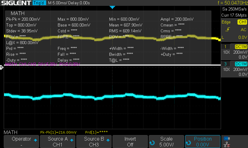
This shows the ripple noise cancellation - the upper and bottom traces are either side of the load, the maths (white trace) shows the difference:
Part of the thermal issue is that the LV power supply actually operates at 32Vdc and not 24Vdc which reduces the SOA below what's needed. So burning about 4W with a resistor and LM317 would work to reduce the noise and lower the the thermal issue back to the model's 24V.
The same is true with the HV although a little more complicated.
So the bode plot - With some tightening of bolts it can typically last long enough to get a bode plot or two before we start getting close to 190-200mA which I've set as my SOA max for now.
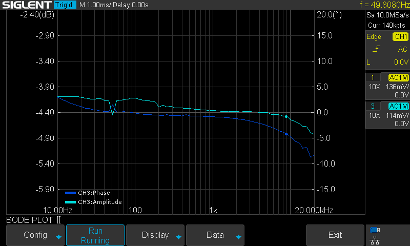
That's one side of the channel as I can't bode plot the difference of two probes. That's a pretty flat curve at -0.7dB across 10Hz to 20KHz. Also note that with a balanced source, the output would be louder still. (also note no snubber present currently with just the RCRC filters)
I had a listen using the test speaker in parallel with the 55R load (Ie it's driving 26R load 😀). There's still mains hum and some DC offset but the sound is good. I think the next step is to target the heating issue and the DC offset.
The heating issue is starting to calm down a little - it takes longer for the NPNs to heat up. The phase change compound required 60degC to sort itself out and the MJE243G has a max of 150degC. The issue here is the SOA for 30Vdc is 200mA for dc operation which may not allow the temperature for long enough to phase change.
I'm thinking a LM317 to create a 20V regulated load would be good at that point the SOA can deal with 600mA max for DC operation. That would also reduce the mains hum noise.
Next up would be the HV supply with a 317 although it would drop the voltage a little we have enough for the 12BH7A-STR to produce a good sound.
The 317 would be cheaper in the initial stages compared to to a 3075 for this initial phase given I need a voltage regulator for each of the floating power supplies.
Last edited:
I've started to think more about targeting the ripple with some Maida LM317 style regulators. This is my initial design I'm just starting to model. The downside is that L2 mosfet is £30 a piece (RDSon is in the mOhm), however for modelling this will do as the model seems relatively well behaved.
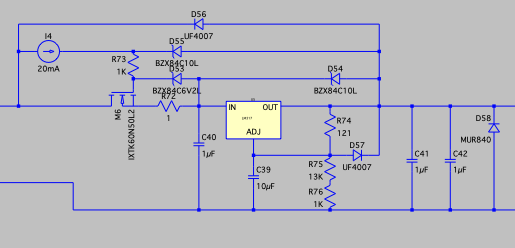
I'll see how the LTSpice FFT turns out. The current source I think will be altered to be a simple CCS running 5-10mA for efficiency.
I'll see how the LTSpice FFT turns out. The current source I think will be altered to be a simple CCS running 5-10mA for efficiency.
I've almost got my maida working - it's been a learning experience.
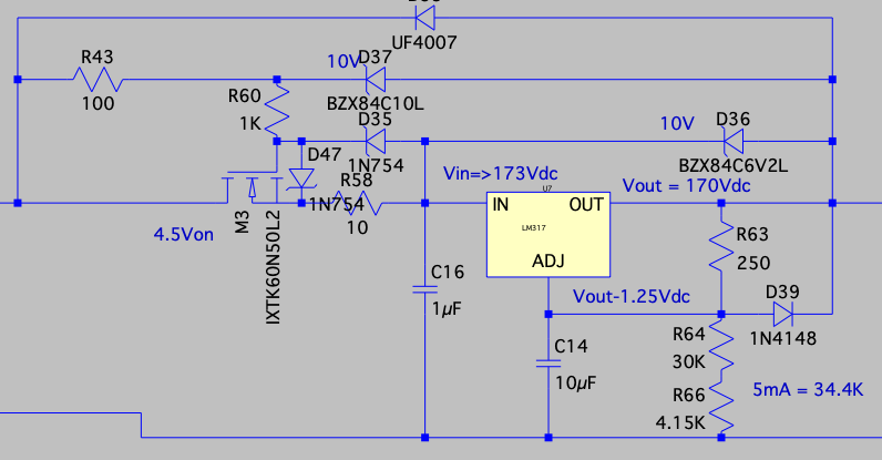
With different components, the required minimum operating voltage drop across each component varies which changes all the values. Also as we only have a small headphone sized voltage swing and a RCRC ahead of the regulator the amount of voltage drop doesn't need to be too high. The main drops are 4.5V min for the mosfet and 3V for the LM317.
The top UF diode prevents reverse polarity across the regulator.
R43 (or a CCS) ensures that the zener D37 has enough current to operate. It also sets the position with that zener of the bubble that the regulator sits in under the input voltage. (you'll also need to sort out the voltage reference divider R63,R64 and R66 for the output voltage to match up within that bubble). The diode D73 should be specced to operate at 10-25% of it's rating. I can see this being requiring a bit of testing with the physical diode.
On startup and a short R43 sees current and the modelling shows this - on a short at full voltage that's going to be quite a current.
R60 is a grid stopper, to filter out the high frequency noise.
D47 is a Vgs positive safety - a LTSpice current source starts at power on and therefore provides a positive base voltage initially. I'm modelling this as a belt and braces (I'll add another across the mosfet source and drain).
D35 pulls the Vgs down to limit on short (startup too)
Mosfet - 4.5V starting voltage, a range of ~5Vgs to 9Vgs means we can use R58 as a voltage regulator, currently this is set to 10R. The mosfet has a <100mRon. It's a 500V 60A piece but for now it will do for modelling given it's hellishly expensive.
So we need at least 4.5V (including any audio noise) across the mosfet.
The LM317 sits in a 10V bubble created by the maximum voltage difference between Vin and Vout set by D36.
There is a stability 1uF cap on the Vout and a bypass cap C14, to stabilise the regulation. For this reason the Vadj needs to protected - this why we have D39 so when the system shuts down C14 does remain charged at high voltage - destroying the LM317. It should be said the same occurs for C16 but D36 also provides protective draining for that.
The voltage divider R36, R64 and R66 (variable) provide the output reference at the required Vadj = Vout-1.25Vdc. Things to note a current source provides the internal LM317 1.25V voltage reference. This is only reliable if the LM317 is on thus the 10uF is charged by the ADJ output and the current coming across R63.
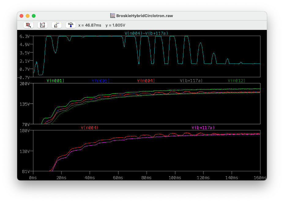
The model below still has some flaws - namely the voltage drop out of the LM317 isn't correct yet but I wanted to show the results so far from LTSpice:
Below the drop out voltage impact - so I need to short out the voltage:
With different components, the required minimum operating voltage drop across each component varies which changes all the values. Also as we only have a small headphone sized voltage swing and a RCRC ahead of the regulator the amount of voltage drop doesn't need to be too high. The main drops are 4.5V min for the mosfet and 3V for the LM317.
The top UF diode prevents reverse polarity across the regulator.
R43 (or a CCS) ensures that the zener D37 has enough current to operate. It also sets the position with that zener of the bubble that the regulator sits in under the input voltage. (you'll also need to sort out the voltage reference divider R63,R64 and R66 for the output voltage to match up within that bubble). The diode D73 should be specced to operate at 10-25% of it's rating. I can see this being requiring a bit of testing with the physical diode.
On startup and a short R43 sees current and the modelling shows this - on a short at full voltage that's going to be quite a current.
R60 is a grid stopper, to filter out the high frequency noise.
D47 is a Vgs positive safety - a LTSpice current source starts at power on and therefore provides a positive base voltage initially. I'm modelling this as a belt and braces (I'll add another across the mosfet source and drain).
D35 pulls the Vgs down to limit on short (startup too)
Mosfet - 4.5V starting voltage, a range of ~5Vgs to 9Vgs means we can use R58 as a voltage regulator, currently this is set to 10R. The mosfet has a <100mRon. It's a 500V 60A piece but for now it will do for modelling given it's hellishly expensive.
So we need at least 4.5V (including any audio noise) across the mosfet.
The LM317 sits in a 10V bubble created by the maximum voltage difference between Vin and Vout set by D36.
There is a stability 1uF cap on the Vout and a bypass cap C14, to stabilise the regulation. For this reason the Vadj needs to protected - this why we have D39 so when the system shuts down C14 does remain charged at high voltage - destroying the LM317. It should be said the same occurs for C16 but D36 also provides protective draining for that.
The voltage divider R36, R64 and R66 (variable) provide the output reference at the required Vadj = Vout-1.25Vdc. Things to note a current source provides the internal LM317 1.25V voltage reference. This is only reliable if the LM317 is on thus the 10uF is charged by the ADJ output and the current coming across R63.
The model below still has some flaws - namely the voltage drop out of the LM317 isn't correct yet but I wanted to show the results so far from LTSpice:
Below the drop out voltage impact - so I need to short out the voltage:
So with the Maida working with the snubbers in place the model shows:
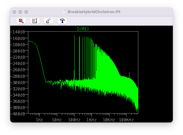
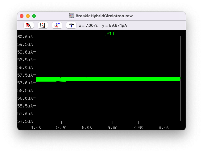
So that is looking good in reducing the ripple noise for zero signal.
So that is looking good in reducing the ripple noise for zero signal.
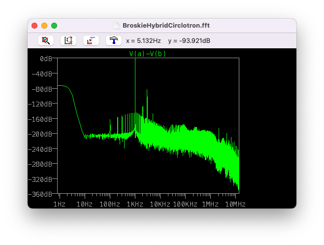
So with zero signal, the FFT now looks like this in LTSpice:
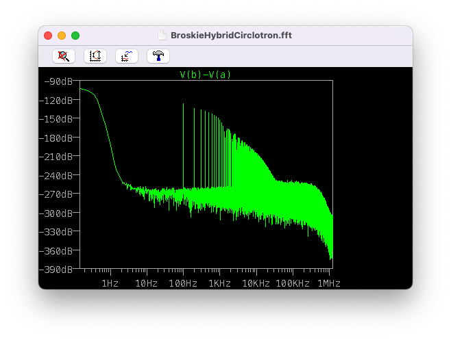
That's better with the V(b)-V(a) rather than I(R1). Now both the mosfet and LM317 are operating when you look at the sim. That's without the current source. It does look like I'm seeing some diode switch harmonic noise still.
Also some good news this morning - I've been offered a new job which should help this move forward a little.
Update - I now have regulated spice model with LT3080s and a Maida LT3080. It's running but with the HV in a small schematic gave about ~16mV ripple (<1mA). Will leave the sim running but this is an <1sec running time FFT:
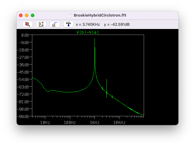
This also has the DC offset mosfets removed for now as they don't get over the gate threshold voltage inreal life. Good as a large DC offset but not when it's under that threshold!
This also has the DC offset mosfets removed for now as they don't get over the gate threshold voltage inreal life. Good as a large DC offset but not when it's under that threshold!
Ok after going back to fundamentals and working through the maida regulator - it makes sense.
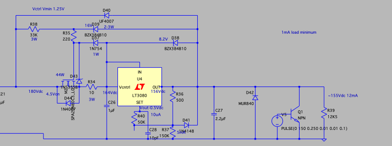
Testing for shorts using Q1+V5 to create a temporary short.
Mosfet gets hammered at 300mA.
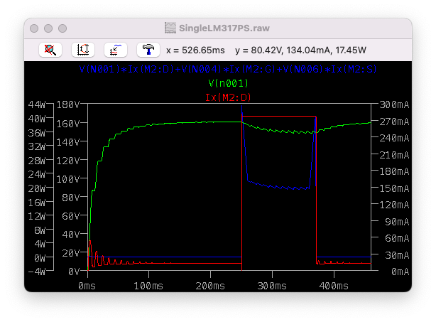
However the regulator would be and D38 would be toast:
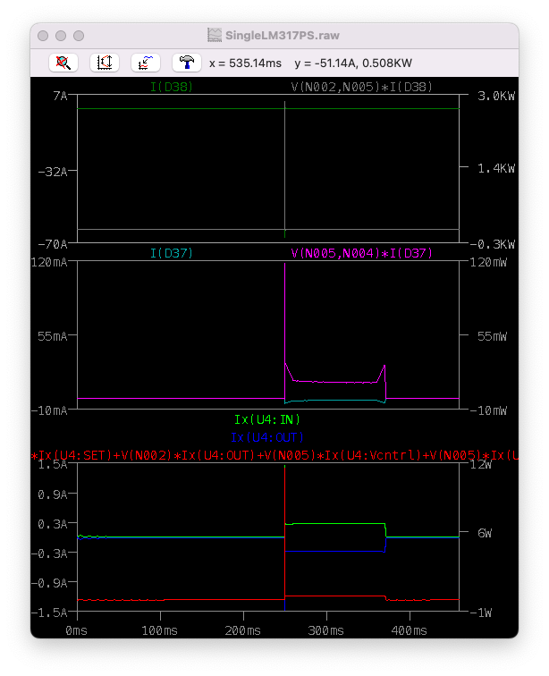
The idea is that the D37 provides a short circuit clamp which saves the mosfet by using R34 as a current limit trigger.
The ripple is starting to look better:
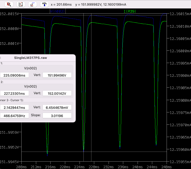
Testing for shorts using Q1+V5 to create a temporary short.
Mosfet gets hammered at 300mA.
However the regulator would be and D38 would be toast:
The idea is that the D37 provides a short circuit clamp which saves the mosfet by using R34 as a current limit trigger.
The ripple is starting to look better:
Last edited:
That spike is caused by the 1uF between the mosfet and the LDO.
Also although it shows as massive ampage, the RMS current is 14A. So as long as the Schottky D38 is a tough little cookie then it shouldn't have a problem. For example a 15V 20A can cope with small 700A spikes: https://uk.farnell.com/vishay/vs-stps20l15d-m3/schottky-rectifier-single-15v/dp/2909680
The LT3080 seems to limit to ~ 1.2A but I'm not sure that's a bang or current limiting.
The sim is starting to look good with the maida regulators in place - for this I'm only dropping about 10-20 volts as the head room required for any amplified signal is only a few volts.
I've set the regulators voltage on the solid state side to 20V and reduced the capacitance on the output and SET pins keeping closer to the application data sheet values. The result is a faster response. The reduction to 20Vdc sees the SOA area current capability rise to 700mA which should really help the issue I have now in real life (current they're being fed 32Vdc).
I've looked at the short circuit issue - in theory I can see a few things. First the pass mosfet gate diode current limiting switch that prevents the gate from exceeding a preset current models to about 300mA max. Second is that Rob Elliot has a lot if great information about pre-regulation with the same issue - on a short the pass device exceeds the SOA. Rob also comments on the use of "VI Limiters" buried in the gate control section of the output devices plus a diode across the power to contain the diode switch on spike destroying the output devices.
This could be used to limit the MJE output device to within it's SOA area - coupled with the reduction to 20V by the regulator could see this work yet and manage headphone plug shorts.
In terms of designing the Maida regulator and points (recording this here so I don't forget) - this is my thinking and yet to be tested with experimentation:
1. Know you Vin - for example 180V
2. Subtract your mosfet drop out voltage so it doesn't drop out under Vin ripple - for example I have 0.5Vpp ripple and a ~5V drop out according to the data sheet. This gives 175V at the source pin.
3. R10 current sense resistor - with 20mA that will drop 2 volts, in theory should control the mosfet Vgs in a short so I've budgeted 6.8V drop across this resistor (ie 68mA) before the Schottky diode conducts.
4. The LDO (or LM317) VIN sees ~170Vdc Vin but that will vary on current.
5. The LDO then sees the voltage set by the Vout side resistor divider that scales the 10uA current source draw from the VSET pin. Mental note here that the VSET is sensitive hence a 10uF cap on the pin and the data sheets states the pin should be guarded by VOUT. This voltage divider has 1mA across it (same as the data sheet). Having the trace with a ground plane would help noise just as an SMPS compensation and feedback implementation in some of SMPS ICs have in their datasheets (TI).
On start R38 must resist the current flowing through D39/D38 etc. Hence the original 470R was not suitable from the results of LTSpice.
In the case of a short the 1uF cap between the mosfet and the LDO remains charged and discharges through the LDO diode (main route) and the LDO VIN up to the maximum voltage. I could place a sense resistor on VOUT and then have VSET cause a shutdown.
I'm going to order a relatively cheap 60V switching bench supply that has current limit and voltage adjust. Although not the best noise levels on the outputs, it will make the development of this and the MJE testing far easier. Up till now the development has been a lightbulb and 240V or 13Vdc non-regulated or current limited. I'll make the regulator on a solder prototype board then ramp up to 60V at which point I can then switch to main supplies.
The power supply I have in mind also connects via USB and there's an open source library to operate it from python for the programmable side (without having to go through two dials). In deciding the most important features - a dedicated current knob, output enable button for those "it's getting warm" moments and also a dedicated voltage knob with voltage and current read outs. It also has some aux outputs for 12V and 3.3/5V. It will do.
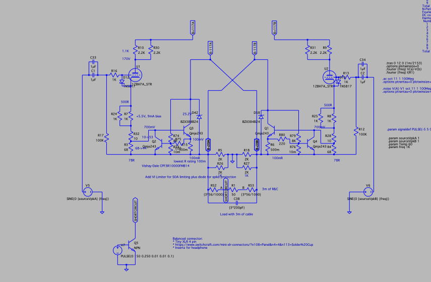
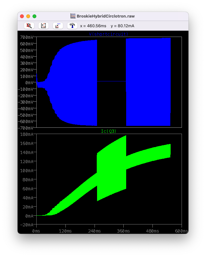
I've started modelling the idea of using VI Limiters, these seem to work well at shutting off the NPNs on short however the power supply is then left without a circuit. The result is a rise to 70V. The impulse spike is removed by the 24V diodes, however the LV power supply sees 70V causing current flow from the LV power supply to the short.
This is an example of when a headphone wire breaks and shorts to ground.
That seems to work nicely and prevents the NPN running off with amps flowing through it. Top trace is the headphone line and the bottom is the current through the output NPN.
Just running one after 1 second - I'll have a look at the impact on the PSs.
This is an example of when a headphone wire breaks and shorts to ground.
That seems to work nicely and prevents the NPN running off with amps flowing through it. Top trace is the headphone line and the bottom is the current through the output NPN.
Just running one after 1 second - I'll have a look at the impact on the PSs.
Last edited:
The parts have arrived - I mess up the quantities on some of some of the resistors but there's enough to build one side totally. I also have some surface mount components.
Now my plan is to use a matrix board, cut out the unused metric pads and then use that to build a PCB. This particular matrix board doesn't have large pads - so the pads have a slightly large gap. I will then attempt to get a 3080 stable on low voltage, move to adding the mosfet on a higher voltage and then scale up the voltage. Plan for cooling is to use a small heatsink for the 3080 which it's probably not going to use much off but for testing it may be more useful to slow down thermal failure. I'll use a block of aluminium for the mosfets.
Just looking at ways to mount a pair of regulators on one board so I can use all the board but not have the heat generating components slap against components that would cause thermal drift and impact the 3080 SET pin.
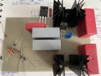
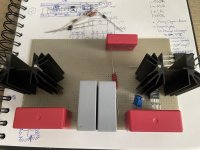
I think the horizontal approach is better. although it doesn't look it, there's corner space for mounting standoffs.
In other news the Tenma PSU arrived. Bad news is it has a minimum 150mA limit.. not 0.. better than nothing and better than trying it direct with the main 177V RCRC from the start 😉
I now need to look at the way the components will be connected - I'd started that (you can see my thinking on the page below the board). In short I need to pay extremely close attention to the SET pin, including putting a 'driven' guard using VOUT for the guard around the SET pin.
Now my plan is to use a matrix board, cut out the unused metric pads and then use that to build a PCB. This particular matrix board doesn't have large pads - so the pads have a slightly large gap. I will then attempt to get a 3080 stable on low voltage, move to adding the mosfet on a higher voltage and then scale up the voltage. Plan for cooling is to use a small heatsink for the 3080 which it's probably not going to use much off but for testing it may be more useful to slow down thermal failure. I'll use a block of aluminium for the mosfets.
Just looking at ways to mount a pair of regulators on one board so I can use all the board but not have the heat generating components slap against components that would cause thermal drift and impact the 3080 SET pin.


I think the horizontal approach is better. although it doesn't look it, there's corner space for mounting standoffs.
In other news the Tenma PSU arrived. Bad news is it has a minimum 150mA limit.. not 0.. better than nothing and better than trying it direct with the main 177V RCRC from the start 😉
I now need to look at the way the components will be connected - I'd started that (you can see my thinking on the page below the board). In short I need to pay extremely close attention to the SET pin, including putting a 'driven' guard using VOUT for the guard around the SET pin.
Last edited:
First attempt at a layout:
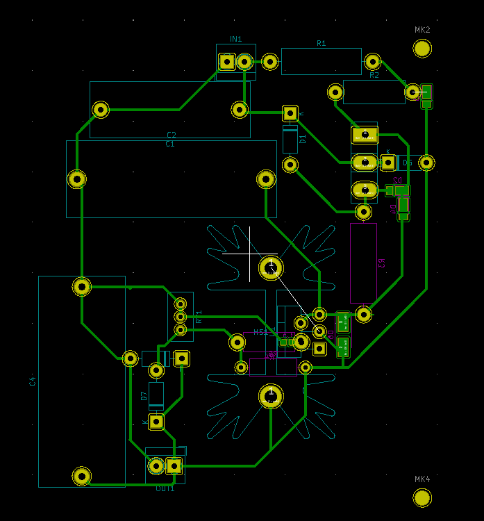
The mosfet will stand off below the board and I've deliberately:
a) Tried to keep the mosfet pin circuitry away from anything such as incoming noise.
b) Tried to keep the SET pin away from any other voltage except VOUT. Here the heatsink is live which means almost 200Vdc. It provides a driven guard, and if I can I will add some wire trace around the pin. The inside of the board has two resistors coming into the pin and a very small SMT cap. If this is not stable enough I will add some VOUT lines to guard but given everything is tied to the pin there's not much more I can do.
c) I've tried not to have a loop antenna, attempted to minimise the input positive area to the mosfet. Same with the outout (I will move the out pins further right.
d) tried to keep the trimmer pot away from the heatsink.
e) tried to keep to one 1/2 of the board hence I can place a second regulator on the other side.
It's difficult being single sided I've had to make use of the gaps made by components like caps and diodes.
So first power up of the 3080 without the mosfet present. I accidentally put a 10V SMBJ instead of a 15V which for the LV regulators will need to be 25V to allow the regulator to operate at 20V. Currently turning the trimmer pot tops out at about 11.6V before the SMBJ starts to conduct.
I currently have a big heatsink on the 3080 for testing, in reality I think a simple bit of aluminium would suffice.
The original RCRC filter in the background attached to the new SMPS regulated power supply and set to 16V. The amp should be operating at 20V for now this is good enough.
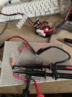
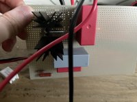
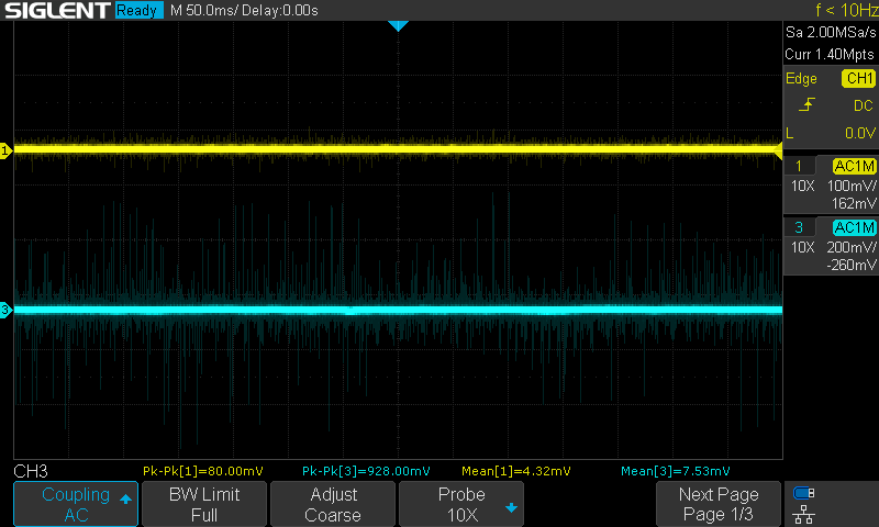
AC coupled, just looking to see what the basic improvement would be. Bottom trace - the signal after the RCRC and at the input pin of the 3080, the top is the output. There's still quite a bit of noise. The mean, although AC coupled dies show a little context - the RCRC filter with the toroid attached still passes about 0.5Vpp through to the amp, so if this is the case it reduces the noise.
The SMBJ doesn't bat an eyelid at 27V given it's a 600W component. There is a 249R resistor as a load for the regulator which got a little toasty. At
Tomorrow I will brave adding the remaining MOSFET etc and start cracking the voltage up towards 60V. However before getting up to the intended 177V, I will need to remove the matrix rings unused between tracks.
I currently have a big heatsink on the 3080 for testing, in reality I think a simple bit of aluminium would suffice.
The original RCRC filter in the background attached to the new SMPS regulated power supply and set to 16V. The amp should be operating at 20V for now this is good enough.


AC coupled, just looking to see what the basic improvement would be. Bottom trace - the signal after the RCRC and at the input pin of the 3080, the top is the output. There's still quite a bit of noise. The mean, although AC coupled dies show a little context - the RCRC filter with the toroid attached still passes about 0.5Vpp through to the amp, so if this is the case it reduces the noise.
The SMBJ doesn't bat an eyelid at 27V given it's a 600W component. There is a 249R resistor as a load for the regulator which got a little toasty. At
Tomorrow I will brave adding the remaining MOSFET etc and start cracking the voltage up towards 60V. However before getting up to the intended 177V, I will need to remove the matrix rings unused between tracks.
Last edited:
- Home
- Amplifiers
- Headphone Systems
- C'est Compliqué - Broskie Hybrid Tube Circlotron