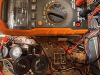
Hello, i’m sorry to be long winded, but I’d like to give detail on my situation. I’m looking for some direction in regards to a Carver MXR-130 receiver I picked up on eBay. I bought it as is and received it in very nice cosmetic condition. I am a diy’er and didn’t want to just power it up not knowing what I may find. I opened up the top of the unit and visually inspected. Other than some really hacked solder joints, I didn’t see anything burned up so I plugged it into a dim bulb tester and powered it up. Nothing smoked immediatel. After it ran for about 10 minutes or so, I removed it from the dim bulb and went to straight power. I connected up a source and some test speakers. It works, and it can play pretty loud. I found the service manual online and found the alignment process and some of the known issues for failure. I addressed a lot of the solder joints that looked shotty, replaced the output relays along with beefing up some various resistors. The voltage adjustment is exactly at 61v on d626 (cathode to chassis.) The idling voltage is where I’m having the issue. The Service Manual calls for 5mv on test points 602 & 601 for the left channel and test points 603 & 604 on the right channel. The bias is only .2mv on the left channel and .3mv on the right. I tried to adjust SVR 501 for the left & SVR 502 for the right channel. The highest I can bring the bias is up to .6mv on the right channel and .4mv on the right. If anyone is familiar with these units, can you please walk me through the troubleshooting steps. It’s most likely that whatever is the issue on the one channel is probably the same issue on the other. Any help would be greatly appreciated. Thank you in advance, Joe
Attachments
my current location doesn't allow access to downloads but if you can get the schematic and post it here... youll be halfway there
Hello, I forgot to mention in my initial post, my DC offset is 0vdc on both channels
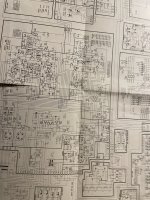
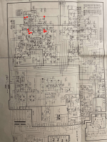
I’ve attached some schematics, hopefully they are readable.
I’ve attached some schematics, hopefully they are readable.
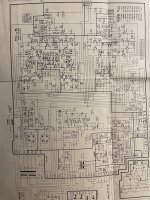

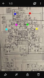
please tell the precise voltage on the location of the red dots... do it for one channel and then the other:I’ve been having a problem uploading pics ever since the platform got updated. Let’s try again
you will write down the volatge at the position with One red dots...then where you have Two red dots and so on...
please lay out your answer like this..
left channel red dot position voltage
1.
2,
3.
4.
right channel red dot position voltage.
1.
2.
3.
4.
thanks
Attachments

please tell the precise voltage on the location of the red dots... do it for one channel and then the other:I’ve been having a problem uploading pics ever since the platform got updated. Let’s try again
you will write down the volatge at the position with One red dot...then where you have Two red dots and so on..
please lay out your answer like this..
left channel red dot position voltage
1.
2,
3.
4.
right channel red dot position voltage.
1.
2.
3.
4.
I never want to leave anyone hanging because the help is greatly appreciated. With that being said I’m working a couple unexpected double shifts at work, I won’t be able to get those points for a couple days for sure but will definitely have later week or the weekend. Thank you so much in advance for digging in with me.
Real quick then I won’t be back for a bit, can you please explain the dots. If we take the right channel, the red dot at R510, do you want from the red dot to ground? Straight down is that from R522 to G? Next, there 3 dots by Q506, is that dot on the collector of that transistor to G or ? The (2) dots below that one, I’m not sure because it looks like there three dots would be common. The 4 dots below by Q518, am I checking from that emitter to G and then R532. Thank you again, Joe
Real quick then I won’t be back for a bit, can you please explain the dots. If we take the right channel, the red dot at R510, do you want from the red dot to ground? Straight down is that from R522 to G? Next, there 3 dots by Q506, is that dot on the collector of that transistor to G or ? The (2) dots below that one, I’m not sure because it looks like there three dots would be common. The 4 dots below by Q518, am I checking from that emitter to G and then R532. Thank you again, Joe
Last edited:
ok...I never want to leave anyone hanging because the help is greatly appreciated. With that being said I’m working a couple unexpected double shifts at work, I won’t be able to get those points for a couple days for sure but will definitely have later week or the weekend. Thank you so much in advance for digging in with me.
Real quick then I won’t be back for a bit, can you please explain the dots. If we take the right channel, the red dot at R510, do you want from the red dot to ground? Straight down is that from R522 to G? Next, there 3 dots by Q506, is that dot on the collector of that transistor to G or ? The (2) dots below that one, I’m not sure because it looks like there three dots would be common. The 4 dots below by Q518, am I checking from that emitter to G and then R532. Thank you again, Joe
sometimes it's easier to just restart.. 😆
please forget everything from the previous post..
take the Black probe of your multimeter and connect it to ground in the circuit... use the RED probe to get voltage readings at the colored dots..
write down the voltage that is present at each colored dot.. please list them here according to color
. just post it whenever you can
Attachments
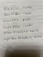
Looks like the red and blue voltage magnitudes are too small, +11.82 vs +16, and -9,69 vs -16 per annotations on the schematic. These voltages are shared for both channels pointing to a common root cause. It would also explain the problem with achieving proper output stage bias.
The next question is why? Going back to the lower right of the schematic (when viewed in normal orientation) shows that these voltages are derived from a zener regulated supply. These are in turn derived from +/- 40 volt supply from a bridge rectifier. Let's check that there is indeed approximately +/- 40 volts present on the nodes as annotated on the schematic.
Assuming for the moment that these are close to +/-40 volts, the most likely culprits are capacitors 622 and 623 as electrolytic capacitors can have poor reliability. Other components in this region of the schematic like the resistors and diodes might also be implicated. If it's none of these then one needs to look for excessive current draw in one of the loads of these supplies.
Please report on the measured values of the +/- 40 volt annotated nodes.

Ok, great as I suspected. Because it's easy, I would measure the resistance of R655 and R657 while in circuit. Power down the unit and wait several minutes for all voltages to decay. Then use a multimeter for measurement. You may have to wait some time for measurements to stabilize be cause of the large capacitors in the circuit. It's likely that you won't see precise measurements while in circuit, but give it a try anyway. Again I suspect them to test good. After this it will be time to investigate the Capacitors C622 and C623.
To do that I would pull one of them out, power up the unit briefly to measure the corresponding for the proper +/- 16 volt reading. If it pops up to the correct level, you have bad caps.
Good luck
To do that I would pull one of them out, power up the unit briefly to measure the corresponding for the proper +/- 16 volt reading. If it pops up to the correct level, you have bad caps.
Good luck
Hello, thank you for the input. I got called out on an emergency call for work this afternoon. I will hopefully get this in the AM
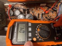
Good evening guys, I stumbled on a dilemma and perhaps someone may be able to clarify. So checking the resistance on R655 and R657 I found the resistors installed in those positions is R655= 680 ohms and R657= 820ohms. I have (2) manuals in possession, one is the free service manual I downloaded off the net and the other is a Carver manual which I purchased. The free manual I have shows the R values I have in those positions. The purchased manual shows R655 should be 270 ohms vs 680 and R657 should be 200 vs 820 ohms. is This a concern? Could this be contributing to the biasing issue? Any thoughts? Thanks for all the help thus far. Joe
That does make things rather confusing! Looking at the design I would think the higher value resistors would be adequate for the application. Can you establish a date on the schematics? The most recent should reflect any design tweets that may have occurred.
That said, I would not change their values till we learn more about what is going on. I would proceed with the temporary pull of one of the capacitors as described previously to further debug.
That said, I would not change their values till we learn more about what is going on. I would proceed with the temporary pull of one of the capacitors as described previously to further debug.
- Home
- Amplifiers
- Solid State
- Carver MXR-130 Bias help!