RocketScientist,
it`s so easy for me to agree with you.
In the Blomley circuit the switching of the output cycles occurs through small signal transistors, faster, more cleanly, being much less disturbed by the output load, but not error free, anyway, amplifying and signal splitting are separated, switching distortion is still present.
Member
Joined 2009
Paid Member
RocketScientist said:And, finally, I'm not sure what you mean Bigun by: "For me the jury is still out on non-swtiching AB." To me you can't use the words "non-switching" and "AB" together. They are mutually exclusive.
I mean by 'the jury is still out' because I haven't seen very much enthusiasm for either approach on the forum here, i.e. neither non-switching ClassB or ClassAG as I've presented it. One exception is the enthusiasm for Steven Dunlap's Krill and hopefully OS will be doing something too.
As a newbie here I find it helpful when a topology has been well explored by people on the Forum as they can bring useful experience on it's benefits and optimization to the table that I don't have. Hence why I'm asking for some help...
And perhaps to be more specific, I'm trying to reduce higher order harmonics, not overall THD 😉
RocketScientist said:I do agree there are plenty of great sounding Class B amps out there. So if you're saying perhaps crossover distortion doesn't matter as much as some think, that's a whole different debate 😉
And what a debate that would be 😀
RocketScientist said:Crossover distortion, in a well designed amp, is typically the biggest distortion left. And the only real way to get rid of it,is Class A. So it depends on if you care about small amounts of distortion.
Many moons ago my first design was a class b amplifier and to be honest I could barely hear the crossover distortion.
Later designs were class AB and they sounded absolutely fantastic with almost zero crossover distortion.
I dont understand the obsession of class A amps when most people couldnt tell the difference between a good class ab and a class a.
You could try enailing someone at EW, they must have coppies somewhere.
I definately have one of the issues with Doug. Selfs design in,its the one with the circuit diagram. Could post it to you.
Cheers Matt.
EDIT: sorry heres the link:
http://www.electronicsworld.co.uk/
I definately have one of the issues with Doug. Selfs design in,its the one with the circuit diagram. Could post it to you.
Cheers Matt.
EDIT: sorry heres the link:
http://www.electronicsworld.co.uk/
nigelwright7557 said:
Many moons ago my first design was a class b amplifier and to be honest I could barely hear the crossover distortion.
Later designs were class AB and they sounded absolutely fantastic with almost zero crossover distortion.
I dont understand the obsession of class A amps when most people couldnt tell the difference between a good class ab and a class a.
My whole point, and that of Douglas Self and others, is due to gm doubling with bipolar outputs you actually can get *MORE* distortion when you raise the bias above the optimum Class B point and the output exceeds the Class A bias setting. Such so called "Class AB" amps are often inferior to a true Class B amp. It's also less efficient than the Class G method being discussed here.
Few realize this, however, because either their amps have too much distortion already and it masks the gm doubling and/or they don't have equipment that can measure down that low. If it's a MOSFET amp, that's a different story. MOSFETs don't have the same gm doubling issue with higher bias.
If you want to keep distortion low you'll have to be a bit more careful with where you are taking rail lifter drive from. Directly from the VAS stage isn't such a good idea. You could try taking drive from the output transistor emitters, or perhaps the driver emitters, so that VAS load won't double when in the outer rails.
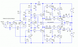
Those 1µF capacitors, C15 and C16, look counterproductive. An RC link might be a better solution if needed. R41 looks out of place, it will take output transistors on the non-driven side into reverse BE breakdown.
Those 1µF capacitors, C15 and C16, look counterproductive. An RC link might be a better solution if needed. R41 looks out of place, it will take output transistors on the non-driven side into reverse BE breakdown.
Member
Joined 2009
Paid Member
megajocke said:If you want to keep distortion low you'll have to be a bit more careful with where you are taking rail lifter drive from. Directly from the VAS stage isn't such a good idea. You could try taking drive from the output transistor emitters, or perhaps the driver emitters, so that VAS load won't double when in the outer rails.
Hi,
Recognizing that this is only a sim...
I did some playing around. The poor signal distortion is not due to loading of the VAS - I tried the sim with the ClassG devices driven directly from their own signal source.
Bigun,
If this is any help, the NAD 2200PE (aka "Power Envelope" series) was one of the better reviewed Class G designs I know of for sound quality. NAD had some quality control issues across their product line around the same time which hurt their reputation, but the 2200PE made Class G work fairly well, although with only 2 output pairs per channel and 95 volt secondary rails, it was a bit under engineered. But you might find some of the Class G implementation useful. Here's a link to the schematic:
NAD 2200PE Power Amp
There's also, of course, the Carver so-called "magnetic field" designs. But the ones I've seen schematics for are even more marginally engineered than the NAD 2200PE above. An example is the 1.0T below, which amazingly, uses a single pair of output devices per channel and supposedly delivers 400w/ch into 4 ohms (which requires over 14 amps of current)!
But it is (more or less) Class G so you might want to check it out:
Carver M1.0t Class G
But it is (more or less) Class G so you might want to check it out:
Carver M1.0t Class G
Member
Joined 2009
Paid Member
Thanks RS, the Carver design helped clarify some of the biassing.
The updated schematic produces comparable distortion to the ClassB reference amplifier and yet when using lower signal levels it is considerably better with predominantly H2 and H3 only. That's just what I was looking for.
I'm not sure what next, I don't feel like building this yet until it's had some further thought and refinement. And I will compare further against two other options (1 - biamp, 2- non switching B).
One thing that is nagging me, how can I get more of that ClassA performance even when it moves into ClassG ?
Attachments
Bigun, you care about the extra power and heat why?
G. Kleinschmidt had a thread for a neat 1000W+ amp that used a floating Class A amp on class B driven rails... from the original idea by iirc Panasonic... seemed like a neat design.
Fwiw, you *do* get the Class A quality as long as you do not switch between rails - the bug in the soup is the hard switching between rails, eh?
_-_-bear
Bigun said:
Hi,
Recognizing that this is only a sim...
I did some playing around. The poor signal distortion is not due to loading of the VAS - I tried the sim with the ClassG devices driven directly from their own signal source.
Interesting. How much voltage drop C to E did you have over the inner devices when in the outer rail? Performance degrades a lot below about 5V Vce or so.
Member
Joined 2009
Paid Member
megajocke said:Interesting. How much voltage drop C to E did you have over the inner devices when in the outer rail? Performance degrades a lot below about 5V Vce or so.
Even though it didn't turn out that the VAS loading was the major culprit, that doesn't mean that it's not causing some distortion. It looks as if cleaning up the biassing helped - there were issues with fast edged current transitions because of how I had things set up. Now it looks much better. Still, the switching transitions of the outer devices can be pretty nasty because when they first come on they have to quickly go from zero to support the full output current, shutting off the diodes in the inner rails as they go.
In terms of Vce, I will have to check the sim again but it isn't very much. Perhaps this is an opportunity for some tweaking. The data sheet for the Fairchild 2SC5200 quotes a lot of specifications based on a Vce of 5V, but I don't think the device performance falls off a cliff until you get quite a bit below that - if I'm understanding the data sheet properly that is ?
Hi Bear,
It does seem that ClassG is more popular with the high power amps where the power savings are really needed. I haven't looked at the floating amp idea, it seems to me that it would be non-trivial in terms of the power supply design and construction. Now that you've reminded me I may look at this approach again though.
The reason I care about the extra power and heat is that I like small and simple amplifiers, as in small boxes, simple thermal management. As a result I've never really considered Class A as an option. But because I'd like to remove the high order ClassB switching distortion (for want of a better description) from my amp at 'normal' listening levels I am exploring some options like this Class G.
Having built some ClassAB designs inspired by AKSA it's not clear that I need anything more in terms of SQ but I've been bitten by the amp bug and find it hard to stop playing with additional ideas.
Bigun said:
In terms of Vce, I will have to check the sim again but it isn't very much. Perhaps this is an opportunity for some tweaking. The data sheet for the Fairchild 2SC5200 quotes a lot of specifications based on a Vce of 5V, but I don't think the device performance falls off a cliff until you get quite a bit below that - if I'm understanding the data sheet properly that is ?
Take a look at the Ic - Vce graph here:
http://www.toshiba.com/taec/components2/Datasheet_Sync/66/7890.pdf
At low collector voltages the current gain drops sharply towards lower voltages, especially at high currents. This causes distortion by increased base current of the output transistors themselves when going into the high rails. Does your simulation show this? IIRC, the speed of the transistor degrades too because of the increasing capacitances.
I have not seen it done (and there might be a good reason why), but what about using MOSFETs for the outer switches? They generally can switch much faster and cleaner than a BJT at high power levels. So I'm wondering if that might solve some of the problems you're seeing in simulation?
One obvious issue is Vgs. So you'd either need to live with the Vgs drop, have still higher rails to drive the gates, or solve it with a clever configuration.
One obvious issue is Vgs. So you'd either need to live with the Vgs drop, have still higher rails to drive the gates, or solve it with a clever configuration.
Lumba Ogir said:Hugh,
many hopeful attempts have been made, in the end doing more damage than good; in practice by the means of an additional error amplifier. The problems are many, accuracy (in time), for instance.
Your opinion? Have you tested every one of them? Listened to every one?
If there was some practical method for solving crossover distortion without much efficiency or other penalty, either all the high-end amp designers would be doing it, or whichever company held the patent would be dominating the market. Neither has proven true. So it would seem none of the "Magic Bias" schemes have really caught on beyond being used as marketing hype by some manufactures.
I didn't patent it, and it is now in the public domain. I think you will find that most designers that can actually design an output prefer their own. This keeps the copying to a low level.
Hi,
The designs I have seen that worked and had low distortion worked by taking the output and feeding it (via a diode) to a drive circuit that runs from the higher voltage rail. A zenner diode defines the level that the rail sits above the output.
An example of this type of circuit can be seen in the TDA7293 data sheet. The circuit we ended up using was significantly different from this as we needed much more power however the approach was similar. I can't show you that as it is a comercial design. It might be worth looking at this type of approach in your simulation.
In the real amplifer, you need to be really careful with the return currents otherwise they will cause big distortion spikes and can make the whole thing unstable.
Regards,
Andrew
Steve,
Don't bother......
I privately emailed Lumba, he has declined to reply, so I believe this question is going nowhere.
Hugh
Don't bother......
I privately emailed Lumba, he has declined to reply, so I believe this question is going nowhere.
Hugh
Steve,
I`ve only listened to Quad, the sound had a nice character, nicer than that of my amplifiers. At the time I believed in the symmetrical topology`s superiority. I was very wrong.
Most approaches rely on part tolerances and require inconvenient component trimming and adjustments changing with temperature and aging. I cannot easily accept the presence of IC error amplifiers.
The challenge lies in arranging a linear load current controlling function and a smooth minimum quiescent current selecting function. Accuracy will also suffer from the inherent time delay.
My opinion on the "magic bias" issue is:
Anyone can claim anything with listening tests. Some love single ended triodes with massive amounts of distortion. So listening tests prove very little about something being superior for anyone but the person doing the listening. One man's pleasure is another man's poison.
For a variety of reasons, like incomplete models, parasitics, EMI induced distortion, thermal distortion, component variations, and the need for convergence, I don't believe simulations are accurate enough to properly represent the small distortions present in even a conventional well designed output stage let alone more complex ones. Even the guys who write the models make it clear they're not a substitute for real world measurements. So comparing simulation data is like deciding what car to buy based on viewing an artist's drawing of each car. It's helpful but an incomplete and inaccurate picture.
So really the only fair means of comparing different output circuits and bias schemes among different people, is with real detailed measurements using equipment of sufficient resolution. Of all the published measured data I've seen, including a bunch of AES papers, manufacture's data, Douglas Self's Class XD data, etc. I've still not seen any bias circuits that match Class A performance when operating outside of the Class A region.
Steve, if you can point me to some measured data that shows your, or anyone else's unusual bias circuit, providing Class A performance at better than Class A efficiency, please provide the link or post the data here?
- Status
- Not open for further replies.
- Home
- Amplifiers
- Solid State
- Can you help understand limitations of ClassA/G ?