Re: Re: Carver 1.0t
Normally the outer (in this case "middle" to be more precise) devices, when they're on at all, should just see approximately the difference between the rails. The Carver is a 3 rail Class G design with 30, 60 and 100 volt rails.
So the middle devices in question (i.e. Q131, Q133) should see the same 30 volts across them as the inner devices. The outer devices (i.e. Q135) have 40 volts across them but there is just one per rail instead of two.
I've seen the multiple pair XO distortion thing argued both ways. I honestly don't know the answer?
Bigun said:
Well a couple of thoughts.
a) the amplifier has to be able to operate at full power and don't the outer devices experience a larger Vce than the inner devices - so to keep a good SOA you want two of them ?
b) ClassAB amps often employ multiple output pairs for higher power handling, but they also benefit from additional devices in terms of lower XO distortion ?
Normally the outer (in this case "middle" to be more precise) devices, when they're on at all, should just see approximately the difference between the rails. The Carver is a 3 rail Class G design with 30, 60 and 100 volt rails.
So the middle devices in question (i.e. Q131, Q133) should see the same 30 volts across them as the inner devices. The outer devices (i.e. Q135) have 40 volts across them but there is just one per rail instead of two.
I've seen the multiple pair XO distortion thing argued both ways. I honestly don't know the answer?
To elaborate a bit on the multiple pair crossover distortion issue... I think it matters if, like Douglas Self, you believe there is ONE optimum bias setting for a Class B amp. If so, and you have multiple pairs, odds are you can only get the bias correct in a single pair and the others will be a bit off--some will be either underbiased, or exhibit gm doubling.
Even if you hand match the pairs, there are still thermal issues. In practice, temps across a heatsink are not constant. Generally the ends are cooler than the center for example. So with multiple pairs they will tend to run at different temps. This further makes exact bias matching and thermal tracking for each pair difficult.
Added pairs also often need larger emitter resistors. And again, this can make the gm doubling problem worse. John Curl has discussed exactly these problems in another thread with his JC-1 amp. He, along with Bob Cordell, discussed how the emitter resistors in the JC-1 for lowest crossover distortion should be 0.1 ohms. But JC had to raise them to 0.15 ohms to keep the amp from blowing up due to current sharing and thermal issues. In the case of a single pair MOSFETs, without a protection circuit, you don't need *any* emitter resistors.
But even if you ignore the above, some argue the lack of matching between output devices across their operating range creates various kinds of dynamic distortion. Others say that might be true, but because each device is handling less current, you end up with a net benefit. Even Self tends to favor multiple devices in what he calls his "load invariant" design because it helps avoid the beta droop and other non-linearities at high current levels.
Self's graphs generally show a lowering of distortion with more pairs but that's only into low impedance loads. Into 8 ohms distortion is often slightly higher than with a single pair.
Added device pairs are also generally more difficult to drive. So, it depends on the topology, driving stage, if you're talking about BJTs or MOSFETs, etc. I'm planning to use double-die power MOSFETs that are essentially a pair of matched MOSFETs in a single package (i.e. BUZ901D) in my next amp. To me they're the best of both worlds. You get almost all the benefits of two pairs, but for bias, Vgs threshold, etc., they behave as a single device.
So I don't think there's a black and white answer. But I hope that helps?
Member
Joined 2009
Paid Member

Member
Joined 2009
Paid Member
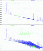
Attached is the FFT profile at 5kHz. I ran a reference TGM amplifier against the ClassGH model for comparison. The Class GH amp is shown by the blue traces and the reference amp by the green traces.
some things to notice
a) Low signal levels (upper plot) it operates in Class A. You can see a nice (blue trace) low order harmonic spectrum. The ClassAB amplifier output is shown for reference (green trace) - lots of switching spikes.
b) Large signal levels (lower plot) it operates in Class GH. You can see a lot of nasty (blue trace) high order switching spikes (mostly out of audible range of course). The ClassAB reference amp doesn't have nearly as much hash.
I don't think there is a simple 'fix' for this, it is a tradeoff of the ClassGH approach and can only be minimized. Nevertheless, it doesn't look too bad, this hash appears only at high frequencies (I used 5kHz to make it visible) and higher signal levels where it will be less audible. For the most part, it will operate in ClassA.
Attachments
Member
Joined 2009
Paid Member
Single Ended Class A - GH
I believe that a big attraction for many in using Class A is going 'single ended' and so this is where I'm exploring next....
I looked at the Class XD idea from Self, and the related ideas from Nelson. My limited understanding says that both ideas, in their basic form, load the output with a constant current source in order to shift current flow patterns in the output stage to achieve SE class A operation. I've read of people doing something like this to commercial op-amps to shift them into Class A.
By adding a current source I can shift my design into SE Class A.
The attached shows a simple implementation. The lower plot shows the currents that are flowing through the (now) three output devices.
The upper device (blue trace) operates in SE class A for low signals (nice sine wave) and Class B at large signals (current clips at zero).
The lower output device (green trace) should be the mirror image, but the 'constant' current source essentially takes away a portion of the current that would normally have flowed this way. There is no current flowing through this device at small signal levels since it now all goes through the 'constant' current source.
The red trace shows the current through the 'constant' current source. At small signals the current is roughly constant. At larger signals when the amplifier moves into Class GH the current source begins sharing current flow with the other output device.
Attachments

Member
Joined 2009
Paid Member
...if you're still with me,
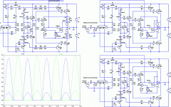
Starting with the last schematic I posted we find that we can remove the lower output device that operates on the inner rails in paralle with the 'constant' current source, leaving just the 'constant' current source load in place. I've shown this in the attachment upper-left corner schematic. Perhaps contra to first impressions this approach still works for large negative signal swings because when the Class G outer devices pull down the voltage on the lower-inner rail this also pulls down the potential at the base of the 'constant' current source thus increasing the current flow. This is now the simplest implementation of the SE Class A-GH amp.
Bear, sorry for the long time waiting, but I have now followed up on your suggestion to look at the floating power supply option - I see this as a means to remove the commutating diodes and hence eliminate the high order harmonic hash. Here's how it unfolds...
In the attachement, upper-right corner schematic I've floated the common-point of the inner-rail power supply off the outer rail devices. An adjustment to the biass puts these outer rail devices into a ClassAB mode of operation. This can be seen clearly when looking at the current flowing through the two outer rail power devices - plottedin the lower-left corner of the attachment. In this case we still have SE Class A operation on the inner rails and the FFT cleans up because we no longer have the switching noise from the commutating diodes or that from the sudden current flows in the outer devices.
We simplify the power supply requirements by eliminating one of the inner supplies, shown in the lower-right corner of the attachment.
I like this !!!!
Starting with the last schematic I posted we find that we can remove the lower output device that operates on the inner rails in paralle with the 'constant' current source, leaving just the 'constant' current source load in place. I've shown this in the attachment upper-left corner schematic. Perhaps contra to first impressions this approach still works for large negative signal swings because when the Class G outer devices pull down the voltage on the lower-inner rail this also pulls down the potential at the base of the 'constant' current source thus increasing the current flow. This is now the simplest implementation of the SE Class A-GH amp.
Hi Bear,
It does seem that ClassG is more popular with the high power amps where the power savings are really needed. I haven't looked at the floating amp idea, it seems to me that it would be non-trivial in terms of the power supply design and construction. Now that you've reminded me I may look at this approach again though.
Bear, sorry for the long time waiting, but I have now followed up on your suggestion to look at the floating power supply option - I see this as a means to remove the commutating diodes and hence eliminate the high order harmonic hash. Here's how it unfolds...
In the attachement, upper-right corner schematic I've floated the common-point of the inner-rail power supply off the outer rail devices. An adjustment to the biass puts these outer rail devices into a ClassAB mode of operation. This can be seen clearly when looking at the current flowing through the two outer rail power devices - plottedin the lower-left corner of the attachment. In this case we still have SE Class A operation on the inner rails and the FFT cleans up because we no longer have the switching noise from the commutating diodes or that from the sudden current flows in the outer devices.
We simplify the power supply requirements by eliminating one of the inner supplies, shown in the lower-right corner of the attachment.
I like this !!!!
Attachments
Member
Joined 2009
Paid Member
Final Version ?
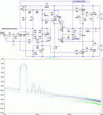
With this new amp there's a lot of current flowing through the inner devices which places a big burden on the drivers and in turn the VAS. So I've flipped the lower driver device up to form a CFP and alleviate the burden. Power dissipation has been minimized by reducing the inner rail voltage to 4V, but this needs to be reviewed in light of the need to keep sufficient Vce accross the output device.
Parts count isn't too bad, not much additional to the reference TGM amp. But I need to look at the 'constant' current source, it may be too basic for best performance and there are some additional power dissipation improvements possible by including some signal dependency to the source (aka Doug Self XD refinements).
The attached shows the current status of this design along with the FFT harmonic plot at 4kHz showing increasing signal levels - predominantly H2/3 as expected from SE Class A.
What else do I need to look at to get this ready for a construction thread ?
Attachments
- Status
- Not open for further replies.
- Home
- Amplifiers
- Solid State
- Can you help understand limitations of ClassA/G ?