Franz,
Then we are in two [at least]. For example, in the past moments I got a lesson... Thanks, Lars and Guido!
Ciao, George
I am learning this way: learning by doing (or learning by error?).
Then we are in two [at least]. For example, in the past moments I got a lesson... Thanks, Lars and Guido!
Ciao, George
Joseph K said:Franz,
Then we are in two [at least]. For example, in the past moments I got a lesson... Thanks, Lars and Guido!
Ciao, George
Hi George,
Looks like there are two lazy-ones here then.... 😀
Thanks for your posts concerning the measurements (and everyone else of course). I was not able to respond earlier, but I see the discussion is still alive!
I wonder how the two inverters at the clock-input in my DAC chip contribute to all this. I've not yet found a way to avoid these. Could it be the waveform is less critical because of this?
I agree the TL431 supply could be improved, some extra filtering would be nice. I hope the "passive" voltage follower with BC550 will contribute something. I regret I don't have the appropriate equipment available other than my ears to make out the difference...
Greetings,
Ray.
Joseph K said:Here it is a pic from an earlier post of mine. A 74F74. I think to discover all the same features here, like that with the AD8561. Assymmetric, rising edge at around 4-5nsec, falling edge much faster, indeed, ringing. Also the level is the same.
Ciao, George
weird, near symmetrical rise / fall but undershoot at falling edge only.....(I know that from optical systems, but electrical systems ?)
cheers
Hi all,
So, after having looked up ALL the kwak pict. postings around here, I finally got it. We just kept on talking beside each other. What You [all] wanted to see is the usual, 50 ohm terminated clock output. Ok, here You are: the very same clock, on the Qout there is a 50 ohm back termination, the other side is terminated at the scope [so there is a heavy amplitude loss, look it up in the original graphs: the output is more than 3.5V]
So, after having looked up ALL the kwak pict. postings around here, I finally got it. We just kept on talking beside each other. What You [all] wanted to see is the usual, 50 ohm terminated clock output. Ok, here You are: the very same clock, on the Qout there is a 50 ohm back termination, the other side is terminated at the scope [so there is a heavy amplitude loss, look it up in the original graphs: the output is more than 3.5V]
Attachments
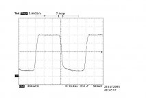
But, I would like to emphasize that it's not the proper way of doing it! That is, it's the proper way of getting the signal out of your clock in practice. But when presenting, the real output signal graphs are those of MINE. THAT is the reality! If You want to see what is happening really in the circuit, you load it as less as possible - with your measurement probe. AND change the different test loads.
Ok, rant mode off, please understand me, I feel like I have lost a full day trying to understand what is wrong with the circuit...🙄 😱
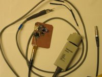
Now I would like to post a pic of the cause of all my troubles:
Ok, rant mode off, please understand me, I feel like I have lost a full day trying to understand what is wrong with the circuit...🙄 😱
Now I would like to post a pic of the cause of all my troubles:
Attachments
Guido,
I think it really works in the same way as You could notice it on the ad8561 output: [where you can see it better, because there are no power supply problems in the way - remember, on the F74 I was intentionally using a weak supply]
The upper half driver is just much weaker than the pull down driver, so the falling edge is much more dramatic, and so generates more bounce. You don't see it very well, because of the probe effects; the weak power supply effects. This is why the edges seem to be more similar.
By the way, your idea of the non-symmetric drive on the comp. inp is for sure valid, anc I checked it [sort of] : according to this, if one takes the signal from the divided up source resistance [shown previously] than it should became more symmetric. I tried it, but no visible effect on the output. The output is affected by the : optional pull-up resistor; the power supply rail values.
Ciao, George
Ray, I don't really got it, the part about your input inverters. If they are outside the chip, much care should be taken there. But once crossed the border, You are in the hands of the designers.. and your chip bypass practice.
The "passive follower" is a Guido design, right? So it should be effective. IF I was right in guessing the problem...
Doh, but where is ELSO? We are talking dirty tech talk about a design, which was optimized by ears! So I hand over...
Ciao, George
The "passive follower" is a Guido design, right? So it should be effective. IF I was right in guessing the problem...
Doh, but where is ELSO? We are talking dirty tech talk about a design, which was optimized by ears! So I hand over...
Ciao, George
Joseph K said:Ray, I don't really got it, the part about your input inverters. If they are outside the chip, much care should be taken there. But once crossed the border, You are in the hands of the designers.. and your chip bypass practice.
The "passive follower" is a Guido design, right? So it should be effective. IF I was right in guessing the problem...
Doh, but where is ELSO? We are talking dirty tech talk about a design, which was optimized by ears! So I hand over...
Ciao, George
Hi George,
Thanks for the detailed measurements. It's a bit hard with my 20MHz scope. But I do have a good probe!
I'm afraid my inverters are just across the border (the DAC is a CD67 SM5872). But it has separate power pins, just for the inverter section, so that is the good news. Never the less, I'd like to see a measurement when the clock is actually in a player, and see how the MCLK or CKO line looks
 .
.You wouldn't happen to have a CD67 or 63 😀 ?
The "passive" follower is indeed of Guido's hand. I hope he doesn't mind me using it with Elso's clock
 ....
....Greetings,
Ray.
Attachments
6h5c said:
The "passive" follower is indeed of Guido's hand. I hope he doesn't mind me using it with Elso's clock
Greetings,
Ray.
Hi
I don't mind at all, kinda hard to limit the use of an emitter follower - the world is full of them 🙂
Hi,
Ehm, I really don't want to insist too much on my previous discourse with a possible optimization for lower phase noise, but I have to admit that me, personally and theoretically got a bit interested in it. And while surfing the net in this direction, I have found something which might be interesting, so I would like to present it to you.
I have found finally the 1/f noise characteristics of the J309 fet, you can find it included here.
I really don't have too much experience in this field, so at first glance i would say not so bad. [As I guessed before]. Though, if we take into account also this..
then it might be really important to search for devices with low noise characteristics in this region. Now, by accident in some physics report in the net, I have found a reference to the BF861C Jfet, which they applied in a ~dozen picovolts/sqrtHz head amp. Which had to be also fast. It's 1/f noise corner freq. is 2-3kHz, which is not bad for a Fet, [against 30/50 kHz with J309], the value at 1kHz is 2nv/sqrt Hz, [it had started from 1nV at 1 Mega] and arrives at 6 nV at 10 Hz.
So, it's not night and day, but not so bad. The transfer admittance is also quite good, 20-30 mS [similar to J309].
Now the bad part of it: hard to find, though it's a Philips, in production.
Ciao, George
Ps.: At this point I would be really curious about the flicker noise of a Mosfet part in a Cmos gate.. 😀
Ehm, I really don't want to insist too much on my previous discourse with a possible optimization for lower phase noise, but I have to admit that me, personally and theoretically got a bit interested in it. And while surfing the net in this direction, I have found something which might be interesting, so I would like to present it to you.
I have found finally the 1/f noise characteristics of the J309 fet, you can find it included here.
I really don't have too much experience in this field, so at first glance i would say not so bad. [As I guessed before]. Though, if we take into account also this..
Close to the carrier, the bandwidth of the filter causes the noise that is produced at the amplifier output to be amplified with a positive feedback that depends on the frequency separation. The gain increases by 20dB/decade.
At some frequency separation flicker noise (1/F noise) will cause phase modulation. To some extent the transistor amplifier is a phase modulator and the current variations through the transistor will change the phase shift through the amplifier very slightly. The flicker noise slopes at 10dB/decade and changes the slope from 20dB/decade to 30dB/decade close to the carrier.
then it might be really important to search for devices with low noise characteristics in this region. Now, by accident in some physics report in the net, I have found a reference to the BF861C Jfet, which they applied in a ~dozen picovolts/sqrtHz head amp. Which had to be also fast. It's 1/f noise corner freq. is 2-3kHz, which is not bad for a Fet, [against 30/50 kHz with J309], the value at 1kHz is 2nv/sqrt Hz, [it had started from 1nV at 1 Mega] and arrives at 6 nV at 10 Hz.
So, it's not night and day, but not so bad. The transfer admittance is also quite good, 20-30 mS [similar to J309].
Now the bad part of it: hard to find, though it's a Philips, in production.
Ciao, George
Ps.: At this point I would be really curious about the flicker noise of a Mosfet part in a Cmos gate.. 😀
Attachments
Hello,
I'm very interested in Elso Clock and I 'd like to know if it can work at 33Mhz?
Anyone have a pcb and mey be some components available to sell?
I'like to realize one of this clocks.
Thans a lot.
Guglielmo
Italy
I'm very interested in Elso Clock and I 'd like to know if it can work at 33Mhz?
Anyone have a pcb and mey be some components available to sell?
I'like to realize one of this clocks.
Thans a lot.
Guglielmo
Italy
KWAK-CLOCK is very good and stable and works just fine at 33Mhz driven by a fundamental crystal.Hello,
I 'd like to know if it can work at 33Mhz?
erm, you do realize that question was posed over 2 years ago right??
I do. But the information about the clock's ability to be driven by 33MHz crystal is still topical and may be useful for somebody reading this forum after that question having been posed over 2 years ago, is it not?
except is he even still using the same clock? its certainly not the same PCB or schematic that you get today. fair comment, but if everyone started answering all the unanswered questions from years past I dont think this forum would be terribly useful
Hello, everybody. I've just try my DIY Kwak-Clock with MP3 player to play WAV file. The result is good (for me). I feed 3.6 - 4 V from Li-Po batt in player, direct to the clock circiut with 330 uF OSCON C coupling. Any suggestion for power supply portion ? ( sorry for poorly english )
- Status
- Not open for further replies.
- Home
- Source & Line
- Digital Line Level
- Can someone send to me the Elso's latest clock schematics (version6)? :)