Hi,
In my search for buffer stage I am currently at Calvin buffer. Lt spice shows nice simulation results with his buffer.
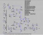
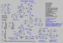
I made a spice file for his servo buffer. Basicaly edited Calvin's original file but of course I ended up in trouble.
I am posting it here,someone smart hopefully can find it out easily.
The problems are
#Not able to get THD output
#Unsure about the servo component values Rv1-Rv5, Q3.
Any help appreciated.
In my search for buffer stage I am currently at Calvin buffer. Lt spice shows nice simulation results with his buffer.
I made a spice file for his servo buffer. Basicaly edited Calvin's original file but of course I ended up in trouble.
I am posting it here,someone smart hopefully can find it out easily.
The problems are
#Not able to get THD output
#Unsure about the servo component values Rv1-Rv5, Q3.
Any help appreciated.
Attachments
Did you try to open it with LT spice or a spice program?I will post a image file too, but was wondering if this is a file issue.
Hi,
the components C5/Rv5 and Cv1/Rv4 are the lowpass filters of the dc servo, defining the lower bandwidth limit.
Two times, because the servo OPAmp is working in noninverting mode here, opposed to the simpler inverting servo one finds more often.
The transistor Q3 inverts the signal though and functions as a ccs that' current is defined by its emitter resistor and the servo's output voltage.
Rv1 is used to take sone heat power losses off of Q3 ... its rather optional here.
jauu
Calvin
Thanks Calvin. What about Rv3?
Will you also please look at my spice file to see why it is not able to detect the out node?
Will you also please look at my spice file to see why it is not able to detect the out node?
Hi,
the node where ´out´ is connected to is also the node ´dc´, hence labelled twice.
LTSpice ignores the out´´.
So either delete the label ´out´, or delete the label dc and rename the ´dc´ label at the servo input ´out´ also.
Rv3 is part of a RC-post-filter for the OPAmp.
The associated C is missing (compare to the circuit on my website, R19/C7).
The RC filter adds a 6dB/oct drop, so that the influence of the servo on the audible range is reduced.
A standard 6dB dc-servo can show considerable output within the audible range.
If You don´t want to use the post filter just omit with the Cap and reduce Rv3 to ~1kOhm.
jauu
Calvin
Calvin that was so useful.
Now everything working.
except these error
Starting Gmin stepping
Gmin = 10
Gmin = 1.07374
vernier = 0.5
vernier = 0.25
vernier = 0.125
vernier = 0.0625
Gmin = 1.08884
vernier = 0.03125
vernier = 0.015625
Gmin = 1.03122
vernier = 0.0078125
vernier = 0.00390625
Gmin = 1.01823
vernier = 0.00520833
vernier = 0.00260417
Gmin = 1.01162
vernier = 0.00347222
vernier = 0.00173611
vernier = 0.00231481
vernier = 0.00115741
Gmin = 1.00877
vernier = 0.00154321
vernier = 0.000771604
Gmin = 1.00673
vernier = 0.00102881
vernier = 0.000514403
vernier = 0.00068587
Gmin = 1.00553
vernier = 0.000514403
vernier = 0.00068587
vernier = 0.000514402
Gmin = 1.00475
Gmin = 0
Gmin stepping failed
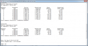
The servo seems like working with offset in 5mv. The issue is THD went up significantly
armonic Frequency Fourier Normalized Phase Normalized
Number [Hz] Component Component [degree] Phase [deg]
1 1.000e+03 1.407e+00 1.000e+00 0.12° 0.00°
2 2.000e+03 4.443e-04 3.158e-04 43.08° 42.97°
3 3.000e+03 2.011e-04 1.429e-04 -147.32° -147.43°
4 4.000e+03 4.585e-05 3.258e-05 37.59° 37.47°
5 5.000e+03 3.055e-06 2.171e-06 116.76° 116.64°
6 6.000e+03 2.511e-05 1.785e-05 -159.04° -159.16°
7 7.000e+03 7.942e-06 5.644e-06 44.54° 44.42°
8 8.000e+03 5.641e-06 4.009e-06 -174.18° -174.30°
9 9.000e+03 8.259e-06 5.869e-06 -165.39° -165.51°
Total Harmonic Distortion: 0.034870%(0.034880%)
Now everything working.
except these error
Starting Gmin stepping
Gmin = 10
Gmin = 1.07374
vernier = 0.5
vernier = 0.25
vernier = 0.125
vernier = 0.0625
Gmin = 1.08884
vernier = 0.03125
vernier = 0.015625
Gmin = 1.03122
vernier = 0.0078125
vernier = 0.00390625
Gmin = 1.01823
vernier = 0.00520833
vernier = 0.00260417
Gmin = 1.01162
vernier = 0.00347222
vernier = 0.00173611
vernier = 0.00231481
vernier = 0.00115741
Gmin = 1.00877
vernier = 0.00154321
vernier = 0.000771604
Gmin = 1.00673
vernier = 0.00102881
vernier = 0.000514403
vernier = 0.00068587
Gmin = 1.00553
vernier = 0.000514403
vernier = 0.00068587
vernier = 0.000514402
Gmin = 1.00475
Gmin = 0
Gmin stepping failed
The servo seems like working with offset in 5mv. The issue is THD went up significantly
armonic Frequency Fourier Normalized Phase Normalized
Number [Hz] Component Component [degree] Phase [deg]
1 1.000e+03 1.407e+00 1.000e+00 0.12° 0.00°
2 2.000e+03 4.443e-04 3.158e-04 43.08° 42.97°
3 3.000e+03 2.011e-04 1.429e-04 -147.32° -147.43°
4 4.000e+03 4.585e-05 3.258e-05 37.59° 37.47°
5 5.000e+03 3.055e-06 2.171e-06 116.76° 116.64°
6 6.000e+03 2.511e-05 1.785e-05 -159.04° -159.16°
7 7.000e+03 7.942e-06 5.644e-06 44.54° 44.42°
8 8.000e+03 5.641e-06 4.009e-06 -174.18° -174.30°
9 9.000e+03 8.259e-06 5.869e-06 -165.39° -165.51°
Total Harmonic Distortion: 0.034870%(0.034880%)
Attachments
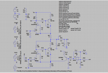
Calvin, I guess that is the issue with Servo( either I made it badly or that is what it is with a servo in this design)!
The RC time of the servo is quite short, 100nF & 10k has an RC time of 1msecond while 1 second (1uF & 1Meg) is common.
With these values I expect significant impact on a 1kHz signal.
Calvin?
Jan
With these values I expect significant impact on a 1kHz signal.
Calvin?
Jan
Last edited:
Jan,
While waiting for Calvin,I did sim with values you suggested.And the THD dropped to original 0.00006 figures.
V-offset between input and output 0.009V ,when I changed the value of R5 and R8 to 6 and 5 ohm to create offset. Without servo measures 0.07V .
While waiting for Calvin,I did sim with values you suggested.And the THD dropped to original 0.00006 figures.
V-offset between input and output 0.009V ,when I changed the value of R5 and R8 to 6 and 5 ohm to create offset. Without servo measures 0.07V .
Attachments
Seems OK now.
Although, 1u and 10Meg is a bit over the top and could cause long slow swings at switch on.
Moral: don't changes things you are not sure you understand 😎
Jan
Although, 1u and 10Meg is a bit over the top and could cause long slow swings at switch on.
Moral: don't changes things you are not sure you understand 😎
Jan
It seems like the servo is affecting the signal. But I am not sure is it a direct effect or indirect due to me picking the wrong components. Hopefully someone knows these stuff better may help out.
Hi,
attached is a circuit, that works as it should.
What seems non optimal in Your schematic?
- R5/R8 seem a bit low in value. The lower values lead to higher idle currents and heat power losses. For loads down to 300=hm (=> 600R balanced) up to 25mA of idle current suffices.
- depending on the chosen input JFET (LSK389 or BF862) choose R1/R6 so that the JFETs idle at 3-5mA.
- choose R8 ~10% lower in value than R5. This can easily be achieved in that You keep R8 = R5 and parallel connect a resistor to R8 of value 10xR5 (or 10xR8, see R12b in my schem).
- choose the servo Caps and Rs = 1µF and 1Meg (don´t know how the other lower values made it into the schem without noticing).
- With high valued servo resistors a JFET-input OPAmp could be a better choice than a bipolar input OPAmp. The new TI OPA140 and OPA141 are high-precision JFET-types ... but the good old OPA134, OPA132 and OPA604 will suffice also.
- choose C4 = 100µF. The post filter´s -3dB freq should be well below the audible range to achieve a noticeable effect.
- Rv2 is way too low and forces the OPAmps output into the supply rail. The optimal value for Rv2 would be chosen so that the OPAmp´s output settles around 0V. As a rough rule-of-thumb procedure choose the current through Q3 = Iidle 1/10. If the buffer idles at say 30mA, choose Iq3 ~3mA. As the OPAmps output holds Q3´s base at ~0V, Q3´s emitter sits at ~600mV. Rv2 then calculates to (Vp-600mV)/3mA, roughly 9V/3mA. So Rv2 should be ~3kOhm in Your schem. In my schem Rv2=R20||R20b. With R20 beeing kind of preset resistor and R20b fine tunes the OPAmps output voltage (and it takes some heat power loss from R20).
- Though the servo can also ´fix´ a certain small input offset voltage I´d suggest to ac-couple the input via a dc-blocking cap. One never knows how the preceding device is built. If it is dc-coupled, utilizing a dc-servo, both devices might ´fight´ for supremacy ... possibly causing oscillation. With a cap the servo can concentrate on defeating only the circuit´s own dc-offset.
- a last note: choose low leakage type caps for Cv1, C5 and C3. In simu, if You use the parasitic parameters of the Caps choose the equiv. parallel resistance no less than 1GOhm. Lower values and the DC-servo seems to loose its servoing capabilities. I´m not sure yet what causes such behaviour and why.
jauu
Calvin
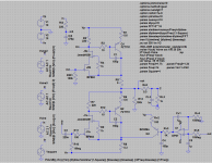
Attachments
Last edited:
Thanks Calvin! That is so nice of you.
What will be the recommended supply voltage for this design. Will 10 V bipolar supply be enough?
Can you please post Fourier components of output too?
What will be the recommended supply voltage for this design. Will 10 V bipolar supply be enough?
Can you please post Fourier components of output too?
Last edited:
Hi,
between +-10V and +-15V should be ok.
Due tio the required voltage overhead of the cascoding JFETs J1a/J2a (J3/J4 in my schem) subtract at least ~4-5V from the supply rail as peak output voltage.
In case of supply rails lower than +-10V consider to omit with J1a/J2a alltogether.
They only make a difference in THD whem driving heavy low-ohmic loads.
If Your load stays >1k then both, cascoded and non-cascoded versions are almost equal.
From the THD figures printed on the schem You can see that the figures remain vanishingly low ... so low that it´d be almost impossible to measure.
Harmonic distribution shows a nice decay towards H2, H3 etc.
So nothing really to post here.
Joachim Gerhard had measured his built of he Buffer and posted the results and found it to be very good.
jauu
Calvin
Removing J3 and J4 seems an attractive option. Any other components needs to be changed out for omitting J3 and J4?
Will it change noise and THD by any means?
Will it change noise and THD by any means?
Hi,
You can omit with the 1k Gate resistors R4 and R9 also.
Since now the max. peak output voltage can reach almost the rails (minus ~1V) and the LSKs as well as the BFs only require ~2V You can get away with only +-6V rails for 2Vrms output.
Make it +-9V to +-12V and You have sufficient headroom for almost any line level load.
Don't go higher for the non-cascoded version, as this could lead to a latch up situation which will destroy the JFET. The LSKs seem to be pretty sensitive in this regard.
I had some simple cascoded JFET Buffers destroyed by this effect.
See the Schottky Diode D1 in my schematic for protection.
Noise isn't affected but by a tiny margin to the better. THD into loads >10k could also be marginally better.
It's into low ohmic loads <<1k and for higher supply rails that the cascoded variant has the edge THD wise.
jauu
Calvin
Last edited:
- Status
- Not open for further replies.
- Home
- Source & Line
- Analog Line Level
- Calvin buffer with servo