Perry,
It will be a couple of days, I've got some different tips coming for my soldering iron (smaller) and I also ordered some various smd resistors and capacitors.
Thanks for your guidance so far.
It will be a couple of days, I've got some different tips coming for my soldering iron (smaller) and I also ordered some various smd resistors and capacitors.
Thanks for your guidance so far.
Attached is the 4150 schematic with the designations and values for the board I have.
Almost all is the same topology except a few differences around the output FETs. My board only use 1 high and 1 low and mine also uses a little different orientation on the rectifier diodes D116, D118, D120 and D122. There were also a few resistors I could not find on mine. I could not edit the lines in the schematic. Also the capacitors are in the correct spot, but even though I left the original values in place (for the sake of order of magnitude), the values on my actual board may be different since most of the resistor values are different from the original diagram.
Almost all is the same topology except a few differences around the output FETs. My board only use 1 high and 1 low and mine also uses a little different orientation on the rectifier diodes D116, D118, D120 and D122. There were also a few resistors I could not find on mine. I could not edit the lines in the schematic. Also the capacitors are in the correct spot, but even though I left the original values in place (for the sake of order of magnitude), the values on my actual board may be different since most of the resistor values are different from the original diagram.
Attachments
Hello Perry,
I've got the "bad" channel ( Ch2), with a drive signal on the outputs and a clean signal at the speaker terminals.
Found a leaking electrolytic C16C on the schematic and changed it.
Found a drive transistor that was giving a 0.35V b to e compared to the other channels 0.67V b to e, so I changed 4 of the 6 npn and pnp drive transistors on that channel, I also noticed that group of 4 transistors getting very hot relative to the good channels.
The last issue is the magnitude of the outputs.
Input: 1kHz sine wave at 1 Vpp
Gain ( Ch 1 and 2) set with channel 2 output at 8 Vpp, channel 1 is 12 Vpp
Gain ( Ch 3 and 4) set with Ch4 output at 8 Vpp, Channel 9.5 Vpp
To achieve these settings Gain pot for Ch1 and 2, is turned about a 1/4 turn more relative to the gain pot for Ch 3 and 4
Vdc on speaker terminals:
1: 13.3 mV
2: 12.9 mV
3: 12.8 mV
4: 12.5 mV
Any ideas as to where I should go from here?
What's the signal level at the output of C1C and C1D equivalents of all channels?
Set the gain when measuring each channel so that you get a consistent level and then compare to the output of the channel being tested.
Set the gain when measuring each channel so that you get a consistent level and then compare to the output of the channel being tested.
I am not sure if I understood correctly, but what I did with meter set to Vac with secondary ground as reference I checked voltage at the output of C1n (n=1 to 4 or A to D in the 4150).
Each two channels 1,2 and 3,4 have one gain pot per pair.
Ch. 1: gain set to 0.5 Vac output 31 Vpp.
Ch.2: Had to increase gain from 0.2 Vac to 0.5 Vac output 31 Vpp
Same trend for Ch3. and Ch.4
So, when the output of C1n for each channel matches, the output at the speaker terminals are the same for those two channels. But the shared pot between the two channels has to be adjusted so that the output of C1n is the same.
When C11 is 0.5 Vac then C12 is 0.2 Vac
When C13 is 0.5 Vac then C14 is 0.3 Vac
Last edited:
What I wanted you to do was to match the input to the 4050 driver IC to see if the gain from there to the output was the same.
If you want to use 1/2v, that's fine. If you set the input to the 4050 to 1/2v (varying the input from the source or gain to get it there), does each channel have the same output level with the 1/2v input?
I'm trying to determine if all class D circuits have the same gain.
If you want to use 1/2v, that's fine. If you set the input to the 4050 to 1/2v (varying the input from the source or gain to get it there), does each channel have the same output level with the 1/2v input?
I'm trying to determine if all class D circuits have the same gain.
The differences could be due to the difference in tracking of the pots, the closeness of the frequency to the crossover or other filters...
You'll have to take it stage by stage to see if you can find the fault.
You'll have to take it stage by stage to see if you can find the fault.
Okay, thank you.
Do you have any schematics that may be close for the preamp section? It uses TL072s as op amps and I believe it is similar to the Class D type 2 amps. It resembles a Planet Audio BB175.4 and obviously the EA4150.
Do you have any schematics that may be close for the preamp section? It uses TL072s as op amps and I believe it is similar to the Class D type 2 amps. It resembles a Planet Audio BB175.4 and obviously the EA4150.
Perry,
I am going to try changing the gain pots as they are not consistent from channel to channel within the same pot.
My question is which series taper should be used on the gain pots?
I am not sure if it was a mistake when assembled, but channel 3/4 is a two gang 20K B series and Channel 1/2 is a two gang 20K C series.
It's probably a mistake.
You can determine the taper by setting the pot to the center position and then measuring from the center terminal to each outer terminal. If the resistance is approximately equal, it's likely a linear taper pot.
The 4150 diagram posted earlier shows B taper for all channels.
You can determine the taper by setting the pot to the center position and then measuring from the center terminal to each outer terminal. If the resistance is approximately equal, it's likely a linear taper pot.
The 4150 diagram posted earlier shows B taper for all channels.
The output of IC301a and IC301b are identical.
The change in the amplitude of the input signal is occurring at the gain pot for Ch 4 (decreased). The attenuation does not occur if the pot is set to either full cw or full ccw, but is present at all points in between.
I have pulled the pot and put a 20K resistor in place of the Ch 4 pot and the attenuation still occurred across that resistor.
I also switched the pots, gang1 and gang2 and no change.
I can place a 10K resistor in parallel with R409 and get the signals on the output of IC302b and IC302a to match pretty close.
When doing the calculations for Vo of IC302, as originally built, with input of 1V both are very close, 3.198 V vs - 3.226V.
What in the gain pot could cause the attenuation of the signal between the output of IC301b and the output of the gain pot?
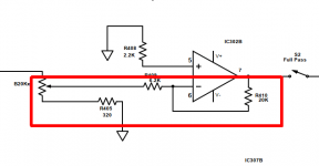
I have drawn the schematic of channels 3 and 4,attached below. Channels 1 and 2 are identical also with the identical problem i.e. Ch 2 and Ch 4 signals attenuated through the gain pot.
There is also a crossover circuit that is not shown, because the problem is occurring before that switch. I may add it in when I get time and post it incase, it might help someone in the future with repairing this type of amplifier as there are several amps, by different names, that appear to use this configuration on the pre-amp.
Thank you
The change in the amplitude of the input signal is occurring at the gain pot for Ch 4 (decreased). The attenuation does not occur if the pot is set to either full cw or full ccw, but is present at all points in between.
I have pulled the pot and put a 20K resistor in place of the Ch 4 pot and the attenuation still occurred across that resistor.
I also switched the pots, gang1 and gang2 and no change.
I can place a 10K resistor in parallel with R409 and get the signals on the output of IC302b and IC302a to match pretty close.
When doing the calculations for Vo of IC302, as originally built, with input of 1V both are very close, 3.198 V vs - 3.226V.
What in the gain pot could cause the attenuation of the signal between the output of IC301b and the output of the gain pot?
I have drawn the schematic of channels 3 and 4,attached below. Channels 1 and 2 are identical also with the identical problem i.e. Ch 2 and Ch 4 signals attenuated through the gain pot.
There is also a crossover circuit that is not shown, because the problem is occurring before that switch. I may add it in when I get time and post it incase, it might help someone in the future with repairing this type of amplifier as there are several amps, by different names, that appear to use this configuration on the pre-amp.
Thank you
Attachments
I have pulled all of those resistors and all are within spec.
Would you suggest just changing the value of R409, to manipulate the gain of the op amp to match outputs?
Changing the value of R409, doesn't explain why the calculated output and the output in practice do not align, but it does seem to at least compensate for the problem.
Would you suggest just changing the value of R409, to manipulate the gain of the op amp to match outputs?
Changing the value of R409, doesn't explain why the calculated output and the output in practice do not align, but it does seem to at least compensate for the problem.
Won't that cause a mismatch at the ends of rotation?
What is the diference in output between the two channels where there is the most difference?
What is the diference in output between the two channels where there is the most difference?
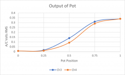
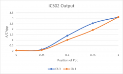
Taken at pins 1 (Ch 3) and 7 (Ch4) of IC302 using a DMM with secondary ground as reference.
Pot Full CCW: Ch 3: 0.05 Vpp, Ch 4: 0.05Vpp
Pot @ 1/2: Ch 3: 1.40 Vpp, Ch 4: 1.01 Vpp
Pot @ 3/4 (greatest difference): Ch 3: 2.54 Vpp, Ch 4: 1.91 Vpp
Pot Full CW: Ch 3: 3.11 Vpp, Ch 4: 3.11 Vpp
I thought that if I graphed the pot position vs output, that if both gangs were possibly different tapers it would show, but they both are trending the same.
Both signals match before entering the pot.
I also previously, disassembled and cleaned both gangs with DeoxIT D5.
Yes, as you mentioned, adding the resistor in parallel with R409, was only successful in matching the signals at 1/2 position of the pots.
Attachments
Last edited:
I am not sure about all frequencies, but I checked it at 40Hz, 500 Hz, 1000 Hz and 5000 Hz. The numbers are not exactly the same, but the trend is the same.
- Home
- General Interest
- Car Audio
- Cadence M4000