You stated that you swapped gain pots and it made no difference. Do both gain pots have the same curve shown on the left, above?
What I did was to disassemble the two gang pot and swap them within the metal case. The reason I swapped them was because the overall resistance of one was 15K while the other read 18K, but it didn't make any difference. They are supposed to be 20 K. Those graphs are with them swapped from there original position.
I ordered some new 2 gang pots that should be here tomorrow. I don't think it will make a difference, but it will rule the pot out.
I appreciate all the help.
I ordered some new 2 gang pots that should be here tomorrow. I don't think it will make a difference, but it will rule the pot out.
I appreciate all the help.
If you have stock of 10k resistors, select some that are the closest to 10k and use them in place of the pot (simulate pot in center position). Does that give you equal gain?
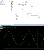
I looked at t he diagram again. Are you sure that the ch3 is accurate?
Are the other two channels like this as well (ch1=ch3 and ch2=ch4)?
The circuit for ch4 looks like a typical circuit but the one for ch3 is odd.
Are the other two channels like this as well (ch1=ch3 and ch2=ch4)?
The circuit for ch4 looks like a typical circuit but the one for ch3 is odd.
Yes, Ch1=Ch3 and Ch2=Ch4. I have gone over it several times. I will look at it again. Which part looks suspect?
They are both identical except for the op amp, IC302b for channel 4, is being used to invert the signal. I assumed for bridging.
Also the resistor configuration and values feeding IC302 between the gain pot and the inputs are different between the two channels.
I am not sure, but I am beginning to think that this imbalance being on both sets of channels was always like this. Maybe a fault in the design? Although Ch2 is worse than Ch4. I've never heard this amplifier before, it was a donor from my brother's pile of amps for me to try and repair and learn on.
If you notice Ch3 has a resistor R307, Ch4 has a spot for that resistor on the pcb marked R407, but it was left out. Same for Ch1 and Ch2 with R207 not installed.
Actually, funny as it may sound, before I realized that Ic302b was set up to invert the signal, I put a resistor in R407 and effectively made IC302b a copy of IC302a (non-inverting). Once I realized my mistake, I changed it back. That's when I started tinkering with the ratio of input to inverting feedback resistance to try and control Vo. I'm still learning and obviously have a long way to go.
Attachments

Last edited:
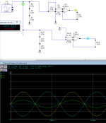
Perry, yes that is exactly what I see on my scope in the real circuit.
Thank you for taking the time to prove that with the simulation. I still need to get a better grasp on how to run a simulation. Which software did you use?
So the options that I can think of are:
Put the cover back on and be happy it is returned to original operation and use an L-pad, for example, to attenuate the output to the speaker?
Rework IC302b circuit to non-inverting output, while adding an auxillary pcb wired in before the gain pot to invert the signal.
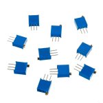
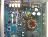
I wonder if separate trim pots, like the ones in the attached picture, could be used to independently control the input gain for each channel? You would have to take the cover off to access them.
If I am out in left field on my thinking or you have another suggestion, please let me know.
Thank you for taking the time to prove that with the simulation. I still need to get a better grasp on how to run a simulation. Which software did you use?
So the options that I can think of are:
Put the cover back on and be happy it is returned to original operation and use an L-pad, for example, to attenuate the output to the speaker?
Rework IC302b circuit to non-inverting output, while adding an auxillary pcb wired in before the gain pot to invert the signal.
I wonder if separate trim pots, like the ones in the attached picture, could be used to independently control the input gain for each channel? You would have to take the cover off to access them.
If I am out in left field on my thinking or you have another suggestion, please let me know.
Attachments
I use an old version of circuit maker. I've had no luck learning any others but there are many better than what I use. Circuit maker has a new free version but it won't run on win7 and I'm not switching to win10.
I don't really encourage re-designing circuits but you could do a few things, relatively easily.
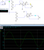
To invert any channel, just pull one terminal of the two input capacitors and swap the positions they go to in the board. You would want to check to confirm that there is no engine noise with the new configuration.
If there is no noise, I'd reconfigure the mixed stages to be like the ch3 circuit.
The trimmers would allow individual level adjustment.
The easiest thing would be the first option, get it working like it was originally and let it go. He brought it in to be repaired, not to be made right. That would justify a higher cost.
An l-pad isn't really an option due to the power level.
I don't really encourage re-designing circuits but you could do a few things, relatively easily.
To invert any channel, just pull one terminal of the two input capacitors and swap the positions they go to in the board. You would want to check to confirm that there is no engine noise with the new configuration.
If there is no noise, I'd reconfigure the mixed stages to be like the ch3 circuit.
The trimmers would allow individual level adjustment.
The easiest thing would be the first option, get it working like it was originally and let it go. He brought it in to be repaired, not to be made right. That would justify a higher cost.
An l-pad isn't really an option due to the power level.
I decided to leave the input as original.
While putting everything back together, as soon as I plug in the cover mounted fan, all leds dim and I lose all output. The protect led does not illuminate.
The fan pin has 5.68 V on the positive terminal. I ran the fan on the external power supply alone at 12V and it ran fine and also quite. I also ran it at 5.6 V it also ran fine, of course it ran slower.
All measurements referenced to chassis ground
Without pulling the board back out and following traces, I believe the fan is feed by the KD600.
E: 5.68 V
C: 5.69 V
B: 6.48 V
The collector of the KD600 appears to be connected to the pin 3 "feed back" of the S494P
Vdc:
1: 2.10
2: 2.11
3: 5.72
4: 13.47
5: 4.85
6: 4.85
7: 1.66
8: 0.02
9: 1.66
10: 4.07
11: 0.12
12: 0.22
13: 1.67
14: 3.04
15: 0.01
16: 5.71
I can get a better pic of the area if needed.
Should the fan be getting 12 V ?
Attachments
1: 1.66
2: 4.13
3: 0.18
4: 0.22
5: 1.66
6: 3.39
7: 0.01
8: 5.70
9: 2.10
10: 2.11
11: 5.71
12: 13.47
13: 4.85
14: 4.85
15: 1.66
16: 0.02
When I referred to pin 3 in #73 it is pin 11.
2: 4.13
3: 0.18
4: 0.22
5: 1.66
6: 3.39
7: 0.01
8: 5.70
9: 2.10
10: 2.11
11: 5.71
12: 13.47
13: 4.85
14: 4.85
15: 1.66
16: 0.02
When I referred to pin 3 in #73 it is pin 11.
- Home
- General Interest
- Car Audio
- Cadence M4000