The amplifier is out of protection and the bad channel output FETs pulled, one of which was shorted. It went out when I checked voltage across R24C with the DMM.
I have taken some measurements with the dmm and o-scope and found some differences in the good channels and the bad channel.
Using the 4150 schematic nomenclature, the values of some of the components are different but I think layout is very close from best I can tell.
Output FETs:
High side
w/o driver board:
G: 26.3Vdc
D: 0 Vdc
S: 26.3 Vdc
w driver board installed:
G: 24.7 Vdc
D: 12.4 mV
S: 24.7 Vdc
Low Side:
w/o driver board
G: -26.3 Vdc
D: 0 Vdc
S: -26.3 Vdc
With driver board:
G: -14.7 Vdc
D: 12.3 mV
S: -24.8 Vdc
On the driver board:
DLI4050:
Good Channel
pin 5: triangle wave 1V pp, 0 Vdc
Bad Channel
5: Distorted Triangle wave riding on -5.14 Vdc
DL201: (good channel followed by corresponding pin on bad channel)
7: square wave 12 Vpp 50% duty 0Vdc
12: noise 0.2 Vpp riding on +5.85 Vdc
9: Triangle wave 0.2Vpp riding on -18 mVdc
4: Triangle 0.1 Vpp riding on 15 mVdc
10:Triangle wave 1 Vpp 0 Vdc
5: Triangle 0.06 Vpp riding on - 5.14 Vdc
Could you please take a look and give me an idea of where to go from here? If how I've noted this doesn't make sense, please let me know and I will try and explain differently.
Thank you.
I didn't think about it earlier but if your circuit is the same as the 4150 diagram, you could simply add the designations for your circuit to the 4150 diagram. Most PDF readers have an option to add text so you can do all of it in the PDF file.
Are the output FETs in both channels where you're reading voltages?
The diagram you posted had too many grounds that didn't seem to correspond to any IC I knew. The ones in the 4150 appear to be an LM319.
You could swap the two LM319s to see if the problem followed the IC.
Are the output FETs in both channels where you're reading voltages?
The diagram you posted had too many grounds that didn't seem to correspond to any IC I knew. The ones in the 4150 appear to be an LM319.
You could swap the two LM319s to see if the problem followed the IC.
The output FETs both low and high were in the "good" channel and the output FETs were removed in the "bad" channel when the above measurements were taken.
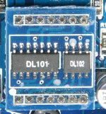
I am not sure about the 14 pin IC, the 4150 has it marked as a DL201 and I found a gut shot of the EA4150D with a DL201, but I never could find any information on that IC. I came up with the pinouts by using the dmm and o-scope. If you could find anything on a DL201 that would be great.
Either way I will try and swap them out and see what changes. I do have a new hot air rework station that I have not used yet.
Attachments
Should I put new output FETs back in the bad channel for future testing or try and get a drive signal first?
I wouldn't use the rework station for ICs. They cause more problems than they solve.
Look at the pin configuration of the 4150 diagram and the LM319.
DL201 is not the original part number. As an example, the parts in a different type of amp, the ICS are a TL072 and an LM319.
Look at the pin configuration of the 4150 diagram and the LM319.
DL201 is not the original part number. As an example, the parts in a different type of amp, the ICS are a TL072 and an LM319.
Attachments
It does seem like the LM319 could be it. My only question about the 319 is that on pins 3 and 8 the datasheet shows GND1 and GND2 respectively, but on my IC I have -6 Vdc on both on those pins, is that okay?
I should just use a soldering iron to remove and install the IC?
Should I install the new FETs back into the bad channel for future testing or try and get a drive signal first?
Thanks
I should just use a soldering iron to remove and install the IC?
Should I install the new FETs back into the bad channel for future testing or try and get a drive signal first?
Thanks
If you look at the datasheet, those 'grounds' are simply the negative supply for the output stage.
I'd try swapping the two DL201 ICs and installing output FETs to see if that solves all of the ch3 problems.
Yes, just a soldering iron. Have you ever removed an SMD IC before?
I'd try swapping the two DL201 ICs and installing output FETs to see if that solves all of the ch3 problems.
Yes, just a soldering iron. Have you ever removed an SMD IC before?
For post 23 I may have not been clear in how I answered that.
The values for the FETs listed in post 21 were only from the low and high side of the bad channel (both FETs removed). The only difference was with the driver board out and the driver board installed.
The other 3 good channels FETs were installed at all times, but all of them were consistent with the readings on the high side of the bad channel.
The only large variation was the voltage on the gate of the low side of the bad channel, with the voltage, not sure of the correct way to say it, becoming 11.6 Vdc more positive or closer to 0 Vdc with respect to the negative rail as soon as the driver board was installed.
The voltage changed with the driver board in because the output of the amp became slightly positive and the driver board was trying to pull the output to 0v by turning the low-side FETs on. That's normal.
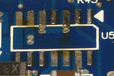
The first thing to know about a low-temp alloy is that you must remove all that you possibly can before reinstalling the IC. The pads have to be absolutely clean and no ripple of remaining solder, like the attached image). I've found this best done with braid and plenty of flux. A bottle of liquid flux is good here, even if the braid has flux in it.
Since you're swapping the IC, you must clean the IC's terminals as clean as you did the board. Do this at a low temperature (start around 200F to see if that will allow the remaining solder to melt). Scuffing (gently) it on a 400 grit abrasive will get you back to bare copper, if you want it that clean.
What's the melting point of the alloy you have?
Apply the paste flux that comes with the alloy to both rows of terminals.
Apply a tiny bit of alloy (1/8", maybe a bit more) to each side and help it melt into the original solder by running the tip of the iron up and down the pins.
Do this to both sides and return to the first side. If you're using enough heat (you'll have to experiment, but less than you normally use to solder) and do it fairly quickly, the IC will begin to move and you can lift it off.
If you have Kapton tape, I'd recommend taping off the area around the IC to prevent contamination if the IC slips or solder drips.
Above, I stated that the action of the drive circuit seemed normal so swapping/replacing the IC may not solve the problem but it will eliminate one possible problem.
Attachments
Last edited:
I appreciate the detailed explanation.
Can you generally idle the amplifier with the LM319 out of the circuit without damaging any other components?
Can you generally idle the amplifier with the LM319 out of the circuit without damaging any other components?
It appears so but it may drive full rail voltage to the speaker terminals. Be careful if you try it.
Swapped LM319s and nothing changed.
What I did notice if I have the dmm set to Vdc and place my probes across R24C I immediately get a good square wave on the output FETs. I also noticed when I do that the amplifier draws excessive current. The B+ series bulb lights up.
What I did notice if I have the dmm set to Vdc and place my probes across R24C I immediately get a good square wave on the output FETs. I also noticed when I do that the amplifier draws excessive current. The B+ series bulb lights up.
What happens if you reverse the probes when you place them on R24C?
Do you have a second meter? If so, does the amp act the same when you do the same thing with it?
Do you have a second meter? If so, does the amp act the same when you do the same thing with it?
Both meters reversing leads makes no difference, square wave both ways.
Both meters set to Vdc
What is different is the magnitude of the peak to peak voltage.
Fluke 187 : 30 Vpp regardless of probe orientation
Fluke 337 : 48 Vpp regardless of probe orientation
Both meters set to Vdc
What is different is the magnitude of the peak to peak voltage.
Fluke 187 : 30 Vpp regardless of probe orientation
Fluke 337 : 48 Vpp regardless of probe orientation
If I remember correctly, you stated that the resistor is within tolerance. Do you have one that you could replace it with?
Yes, it shows to be in tolerance. I don't have any smd resistors. I see they have several kits with multiple valued resistors online. What wattage are typically used?
Is it possible to solder an through hole axial lead resistor to the pads?
Is it possible to solder an through hole axial lead resistor to the pads?
- Home
- General Interest
- Car Audio
- Cadence M4000