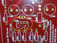
The middle pin of the 7 does nothing
The two sets of the outer 3 are the jFET pins.
One is reversed relative to the other.
holes 3 and 5 are the Source pins.
Turn the left jFET 90° anticlockwise after insulating the Gate lead.
Turn the right jFET 90° anticlockwise after insulating the Gate lead.
You now have a pair facing each other ready for Thermal Coupling.
One of the biggest advantages of the j109 is the Thermal Coupling.
The specified tolerances of matching are not worth buying.
Most pairs achieve much better matching than the tolerance.
But this can still be bettered by hand matching over a range of Id (<Idss).
With (very labour intensive) hand matching and Thermal Coupling you can end up with a better matched pair than using a j109.
Thanks Andrew, I'll take a closer look at the data sheet and the traces on the board for a better understanding. Hopefully Buzz or Spencer will have something I can use.
There is a gentlemen in Swap Meet selling genuine J109's, if you are interested.
Very Much so. Please supply info.😀
Edit: found it - PM sent. Thanks.
Last edited:
Full-fat BA-2
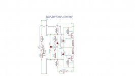
I was playing with the design of a J2-esque/F4 combination for producing comfortably more than 100W into 4 ohms for my Maggies.
But such an approach isn't ideal. When driving the F4 you've got those SemiSouths burning up a lot of heat which is wasted on the F4's 47K input.
Here's another idea which doesn't require the compromises of having the J2-esque also be a good stand-alone amp. While it started as a J2-esque IS, a BA-2 VAS, and an F4 OS, it ends up looking more like a Full-Fat version of a BA-2:
1) rails increased to 46V
2) LTP cascoded
3) LTP CCS changed from single JFET to BJT feedback pair
4) VAS CCS changed from bootstrapped load to BJT feedback pair
5) OS shortened to 4 pairs
Comments appreciated.
Attachments

looks good on paper
also , think about introducing R-C-R , in place of R7 and R34
cleaner ....... everything , for CCS-es
again - look in Babelfish J thread
also , think about introducing R-C-R , in place of R7 and R34
cleaner ....... everything , for CCS-es
again - look in Babelfish J thread
Thanks, ZM & Itsmee.
For adjustability of the CCS(s) I was planning on socketing R17 and R18. But increasing them a bit and installing parallel pots would certainly be easier to adjust....
For adjustability of the CCS(s) I was planning on socketing R17 and R18. But increasing them a bit and installing parallel pots would certainly be easier to adjust....
I'm not fond of sockets, can be tempremental, I'd rather use a multiturn preset.
I prefer paralleling resistors to trim.
I prefer paralleling resistors to trim.
In re-reading the thread from the start (again), I noted there were a couple of side comments on replacing the VAS IRF610 with a SemiSouth, but the actual conversations appear to have happened elsewhere.
Can anyone say more about this?
Can anyone say more about this?
We got to the moon on slide rules and haven't been back since, just go for it...I really can't remember how this ended in this thread 😕
just go for it ; unimportant difference
Help! Got some troubles with my BA2 amplifier. I've set it up in a chassis without the FE. FE is BA3 in a separate chassis set up as preamp, no issues here.
I was able to set bias at the BA2 and could also set offset to 0 V after I modified R25 from 15k to 14k. I use 31 V rails. The build is 3 pairs deep, I've used R .51 3W instead of 1 R as suggested by Pa in his article. As already mentioned I was able to bias (588 mA pro device, could even go higher I`m at 45 degree C) and set offset to zero, let it cook, checked everything after 12 hours --> all good. but then I noticed that I have -4.4V offset at the RCA inputs. When I apply a signal also the output gets offset of 4.4 V positive in this case, but I get the signal without distortion. Zero offset without a signal. I've connected the RCA inputs hot to D and GND to star ground. LS return also to star ground. Star ground is connected to chassis ground by an CL60. I kindly ask for advice.


I was able to set bias at the BA2 and could also set offset to 0 V after I modified R25 from 15k to 14k. I use 31 V rails. The build is 3 pairs deep, I've used R .51 3W instead of 1 R as suggested by Pa in his article. As already mentioned I was able to bias (588 mA pro device, could even go higher I`m at 45 degree C) and set offset to zero, let it cook, checked everything after 12 hours --> all good. but then I noticed that I have -4.4V offset at the RCA inputs. When I apply a signal also the output gets offset of 4.4 V positive in this case, but I get the signal without distortion. Zero offset without a signal. I've connected the RCA inputs hot to D and GND to star ground. LS return also to star ground. Star ground is connected to chassis ground by an CL60. I kindly ask for advice.
That's normal. D+ lives at a voltage close to the Vgs of the P-channel output FETs.
This output stage is expecting to be driven from a cap-coupled FE, which mitigates any issues.
This output stage is expecting to be driven from a cap-coupled FE, which mitigates any issues.
What worries me is that I get positive offset at the speaker terminals once I apply a signal to the input. No signal, no offset at the speaker terminals. Could be an issue with the grounding of the RCA plugs? I‘m clueless…
When I connect FE with the RCA plugs, no matter off or on. I don‘t have any offset on the output of the FE.
When I apply a signal with a signal generator.
In both cases I get positive offset of about 4 V on the speaker terminals.
I try to remove RCA gnd from ground star.
When I apply a signal with a signal generator.
In both cases I get positive offset of about 4 V on the speaker terminals.
I try to remove RCA gnd from ground star.
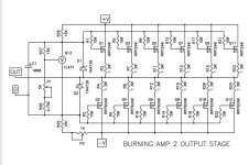
RCA jacks are properly isolated from the chassis? Also the schematic @ post 1,134 has an error, correct one attached.. anyhow. Wouldn't a standalone output stage like this still need some sort of input ground reference? Isn't this flapping in the breeze without the typical 47K-220K resistor from RCA input to ground? Maybe one of these designers will chime in and correct me if necessary..
Attachments
- Home
- Amplifiers
- Pass Labs
- Burning Amplifier BA-2