Glad to hear...https://www.diyaudio.com/community/...ac-using-tda1541a.79452/page-489#post-7814169
it was some issue with the Arduino I2S.h library or the ESP8266 itself. I asked OpenAI ChatGPT what to do, and he/she advised to insert one sampling period delay (buffering the previous sample) in the R channel.
Now both channels are perfectly in sync.
Next action will be to mimic a balanced (dual mono) configuration by adding L+R using the same input (full scale dithered sine and -60 dBFS dithered sine) and see the distortion spectrum, compared to individual channels. Results will follow.
What is the final delay time of sample at output, now same for booth channels?

it was some issue with the Arduino I2S.h library or the ESP8266 itself. I asked OpenAI ChatGPT what to do, and he/she advised to insert one sampling period delay (buffering the previous sample) in the R channel.
ROTFLMAO! 😂
That's just like an AI. Why fix the real problem if we can use duct tape?
Arguably it is sufficient for what you need. But anyone wo uses ESP8266 and Arduino for Audio will have the same issue.
Thor
Use to like going to the part in Krung Thep where all the electronic parts street & mall to walk around. Oh & that's where
I bought my collection of 1541 including a couple of S1's.
I hear then place has turned to ..... censored. Cannot find any good stuff.
What's your take on the Audio scene there including diy.
I'm not really in this, I only know a few farrang into this. I suspect without speaking Thai the entry is not easy.
Thor
ChatGPT noted that this is a workaround and the real reason might be the weakness of ESP8266 vs. ESP32. Anyway, it works for me and I don't want to spend more time on it.ROTFLMAO! 😂
That's just like an AI. Why fix the real problem if we can use duct tape?
Arguably it is sufficient for what you need. But anyone wo uses ESP8266 and Arduino for Audio will have the same issue.
Thor
If only it could roll caps for us ! 😀Wow looks like we can get ChatGPT to help design circuits for us ya. Lol
It is not clever enough yet... 🤔
Ok, I promised the AscenDance version (pun intended).
First draft and it shows both the possibilities and penalties in complexity on really going out on a limb....

There are few little things here that may be worth explaining.
First, I decided to switch the DEM SYNC to a balanced Grundig Circuit. Reason is, that in the sim the very "light handed" version can be instable at higher speeds. In the end when the oscillator circuit has one transistor shut off and the other at maximum current current flow stops. Being balanced, there is no net current injected. The two TDA1541 run at opposite polarity, this means any switching noise tracked into the power supplies happens at 1/2 the current of simultaneous switching and twice the frequency. In my books a "good thing".
The TL431 circuit around the super capacitors is a forced protection/balancer, using a style of circuit normally seen in the regulation of SMPS. The capacitor from anode to ADJ sets the AC loop gain, 1K & 100uF gives a 1.5Hz turnover. The 22k resistor makes sure that each 431 only turns on with typically 5.2V across the series connected block. That is, as long as things are normal, the 431 is actually off. If it turns on it will progressively not try to regulate anything above 1.6Hz. The 47R resistors limit the current in each TL431 to 60mA, appropriate for SMD versions. If TH TO-92 is used, the resistors can change to 27R.
There are a few resistors to balance out all currents to pretty much net zero. The analogue voltage comes from 30V DC, the analogue stage will run from +/-15V and be no-buffer balanced with a passive LC filter as output. Nope, no Op-Amp's (I think). Each channels output stage is current steering and needs around 50mA.
There is technically no negative regulator. Instead we regulate DGND to 5V higher than the -5VD line. The 150R resistor makes sure to draw enough current that there is always some current flow. The +5V line is regulated to be 10V higher (under load) than the -5V line.
This allows us two completely floating voltages of appx. 45V and 15V DC giving respectively 30V & 10V well regulated and passively filtered supplies.
The 317's use a trick to limit current used long ago for battery charging (Lead Calcium or Acid trickle charging), with current limited to ~ 0.5A the charging time is around 120 seconds or 2 minutes. So this DAC will have a significant warm up time.
I'll sit on this for a few days to see if any more ideas percolate and then start a PCB Layout in Altium.
Thor
First draft and it shows both the possibilities and penalties in complexity on really going out on a limb....
There are few little things here that may be worth explaining.
First, I decided to switch the DEM SYNC to a balanced Grundig Circuit. Reason is, that in the sim the very "light handed" version can be instable at higher speeds. In the end when the oscillator circuit has one transistor shut off and the other at maximum current current flow stops. Being balanced, there is no net current injected. The two TDA1541 run at opposite polarity, this means any switching noise tracked into the power supplies happens at 1/2 the current of simultaneous switching and twice the frequency. In my books a "good thing".
The TL431 circuit around the super capacitors is a forced protection/balancer, using a style of circuit normally seen in the regulation of SMPS. The capacitor from anode to ADJ sets the AC loop gain, 1K & 100uF gives a 1.5Hz turnover. The 22k resistor makes sure that each 431 only turns on with typically 5.2V across the series connected block. That is, as long as things are normal, the 431 is actually off. If it turns on it will progressively not try to regulate anything above 1.6Hz. The 47R resistors limit the current in each TL431 to 60mA, appropriate for SMD versions. If TH TO-92 is used, the resistors can change to 27R.
There are a few resistors to balance out all currents to pretty much net zero. The analogue voltage comes from 30V DC, the analogue stage will run from +/-15V and be no-buffer balanced with a passive LC filter as output. Nope, no Op-Amp's (I think). Each channels output stage is current steering and needs around 50mA.
There is technically no negative regulator. Instead we regulate DGND to 5V higher than the -5VD line. The 150R resistor makes sure to draw enough current that there is always some current flow. The +5V line is regulated to be 10V higher (under load) than the -5V line.
This allows us two completely floating voltages of appx. 45V and 15V DC giving respectively 30V & 10V well regulated and passively filtered supplies.
The 317's use a trick to limit current used long ago for battery charging (Lead Calcium or Acid trickle charging), with current limited to ~ 0.5A the charging time is around 120 seconds or 2 minutes. So this DAC will have a significant warm up time.
I'll sit on this for a few days to see if any more ideas percolate and then start a PCB Layout in Altium.
Thor
We could piggy back a Core pcb daugther ( that is almost finish) with the same core sharing the supply of the mother board (extended core with supply) as I shown in PM ?
Edit : I see, all the suply is different, so not feasible. I wonder if I should continue the standalone one, better to jump direct on a 2 IC version directly made by you than mine with your advices 🙂 ? And no doubt Altium IS the pcb cad Soft. Calculating impedance of tracks is a nigthmare I find in Kickad... as doing clean pads for decoupling with vias.
Edit : I see, all the suply is different, so not feasible. I wonder if I should continue the standalone one, better to jump direct on a 2 IC version directly made by you than mine with your advices 🙂 ? And no doubt Altium IS the pcb cad Soft. Calculating impedance of tracks is a nigthmare I find in Kickad... as doing clean pads for decoupling with vias.
Attachments
Last edited:
We could piggy back a Core pcb daugther ( that is almost finish) with the same core sharing the supply of the mother board (extended core with supply) as I shown in PM ?
No, this will be deliberately split into +/-15VA and +/-5VD which is more doable on a balanced setup. It will also include the analogue stage on board.
As I do not have the time to deal with supporting PCB's I will consider if I make the actual PCB public domain.
I will make a PCB because that is now well past veroboard, kapton and copper tape.
Edit : I see, all the suply is different, so not feasible. I wonder if I should continue the standalone one, better to jump direct on a 2 IC version directly made by you than mine with your advices 🙂 ?
The argument up to now for the single was that TDA1541 are rare, expensive and so on.
I now have enough donor CD players to not mind.
But I think most people would probably prefer a single TDA1541 PCB without super capacitors and with limited complexity, but as high performance as doable within this set of limitations.
Thor
Thanks a lot to @ThorstenL and all the contributors for sharing their valuable knowledge and practical information for building this TDA1541A DAC.
How the I/V stage presented in post #9243 can be used in this differential version? is it sufficient to simply remove the phase splitter and duplicate the ciricuit?First draft and it shows both the possibilities and penalties in complexity on really going out on a limb....
Last edited:
LOLIf only it could roll caps for us ! 😀
It is not clever enough yet... 🤔
Thailand overall is a wondering country. Enjoy your stay there.I hear then place has turned to ..... censored. Cannot find any good stuff.
I'm not really in this, I only know a few farrang into this. I suspect without speaking Thai the entry is not easy.
Thor
Cheers
Which version do you have?Wow looks like we can get ChatGPT to help design circuits for us ya. Lol
I find the 'teaser' to be helpful with absolutes, calculations for example - but is unashamedly brash with its 'making **** up'. When you question it with a 'fact' which runs counter to the 'output' it retracts, and supports the 'calling out' and offers to 'be better next time' - all that, only to do it again.
Yep, free version YMMV.
Last edited:
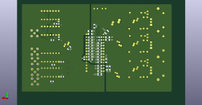
you have the decoupling caps under the chip and facing toward chip centerline now (I like it but why?).. assume AOL/R skirt around the IC as per T's CD-77 v7.0 layout (?) - you really might be the guy with the PCB ..We could piggy back a Core pcb daugther ( that is almost finish) with the same core sharing the supply of the mother board (extended core with supply) as I shown in PM ?
Edit : I see, all the suply is different, so not feasible. I wonder if I should continue the standalone one, better to jump direct on a 2 IC version directly made by you than mine with your advices 🙂 ? And no doubt Altium IS the pcb cad Soft. Calculating impedance of tracks is a nigthmare I find in Kickad... as doing clean pads for decoupling with vias.
Last edited:
I find the 'teaser' to be helpful with absolutes, calculations for example - but is unashamedly brash with its 'making **** up'. When you question it with a 'fact' which runs counter to the 'output' it retracts, and supports the 'calling out' and offers to 'be better next time' - all that, only to do it again.
I tried it multiple times on very simple, fact based stuff that I already knew the answer to. Google was actually more useful.
I tried a programing problem that had me stuck, it went into all sorts of BS. Google found me an article reminding me that 8 bit Micro C compilers do not handle longint data types In calculations directly and truncate the top 16 MSB.
ChatGPT? Artificial, yes. Intelligence? About 1/100 of Googles algorithm.
Supposedly it improves with time. I don't see it. I can only definite it as the biggest waste of my time each and every time.
Thor
ChatGPT echoes what it has read on the internet. If it has no information on the subject, it compiles the answer where the main object is it should be grammatically correct, and "serious and credible" sounding.
Since ours is a specific field (I mean my case with ESP8266 and I2S), probably it could find some relevant information and previous work documented.
(I once asked how many funnels the Titanic had. The answers varied between 4 and 26. Each with an utmost polite manner).
Since ours is a specific field (I mean my case with ESP8266 and I2S), probably it could find some relevant information and previous work documented.
(I once asked how many funnels the Titanic had. The answers varied between 4 and 26. Each with an utmost polite manner).
Sure, just because it takes real intelligence to discriminate the content of what one "reads".Google was actually more useful.
An algorithm will never be able to do that.
Never.
IMHO
you have the decoupling caps under the chip and facing toward chip centerline now (I like it but why?).. assume AOL/R skirt around the IC as per T's CD-77 v7.0 layout (?) - you really might be the guy with the PCB ..
It is progressing everyday, don't focus on what I posted above.
And changes migth happen with Thorsten Losch ideas and Icsaszar work.
I tried to ask CHATGPT about op amps or what the best dac and I was disapointed by the answers and I almost was out to learn bag pipes because of it!
Last edited:
- Home
- Source & Line
- Digital Line Level
- Building the ultimate NOS DAC using TDA1541A