Interresting , what do you think will be the issues having a to quick slew rate ?"Stopped clock" is a great idea.
I've implemented it with no observable sonic improvements.
You'd still need slew-rate attenuation on the digital input side.
This is the consequence of the logic type used inside the chip.
.
thanks 🙂
looks good?
Remind me when conversion starting for already loaded data, LE rising edge?
+Nevertheless, I will use a copper heatsink, because it is cool (pun intended), and it provides shielding against EMI. The heatsink should be connected to GND.
Yes
HiI measured the actual currents right at the supply/GND pins.
+5 V: 30.0 mA at -2 mA output current. 25.9 mA at -4 mA output current. 34.3 mA at zero output current.
-5 V: 39.2 mA fixed
-15 V: 26.45 mA fixed
AGND: 1.93 mA fixed
DGND: 29.55 mA fixed
I double checked the AGND current.
Could You please post the diagram of power supply connections?
It seems that A and D suply are independant?
Are You used 2mA current injection on Iout pins?
Thanks 🙂
@icsazar,
It is Thorsten shematic you measured or raw with just the V input pins decoupled?
It is AC, at pin 14 dgnd, where the current are going to from pin 14 ? In the Ic, on the pcb ?
It is Thorsten shematic you measured or raw with just the V input pins decoupled?
It is AC, at pin 14 dgnd, where the current are going to from pin 14 ? In the Ic, on the pcb ?
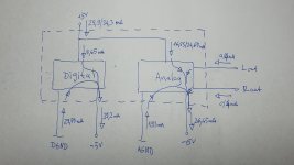
I built a standard series regulator for +/- 15V and +/- 5V. These regulators have a common star GND. The AGND and DGND are independently connected to this common star GND. The measurements were taken by disconnecting the +5V, measure the current flowing into pin 28, then doing the same with pin 26 (-5 V) and pin 15 (-15 V). Then I disconnected AGND (pin 5), measured the current, and did the same with DGND (pin 14). This way the current flowing in or out each pin was measured independently. See the jumpers at my picture of the test setup.

As it was stated before (by Thor and others) the +5 V serves for both analog and digital supply, unfortunately. It would have been better if Philips engineers decided on a separate +15 V for analog supply. Probably there weren't enough free pins 😏.It seems that A and D suply are independant?
Are You used 2mA current injection on Iout pins?
I do not use 2 mA current injection in my tests. But I will use in the final DAC. This test setup is dedicated for measurements an trying various ideas, the final DAC will be for listening to music.
What signal did you inject into the 3 I2S pins ?
Seems AGND is the reference pin for the pcb and internally analog current flows internally through digital ground then in pin 14 towards pcb ?
WHich I try to understand is how flows the differents AC loops both and on pcb, during music operation.
What is your point about that, please?
Edit & decoralated : I do remember at theend John gave up attenuation on the Bck line or the whole I2S inputs ?
Tha's funny if we arrive to close pcbs but differents decouplings, same-same but different as Thaïs say ! I focus on last Thor's shematic, but it willl be cool to see at the end if differences can be checked with the ears between two close DAC with the same I/V.
Last edited:
Today I spent some time for measuring THD vs temperature. I used a freeze spray, a hairdryer and an IR handheld "gun" thermometer. I measured THD at full scale and at -60 dB. The free air temperature of the TDA was 49 °C. I freezed it to +15 °C and heated up to +60 °C. The ambient was 24.5 °C.
The result is surprising even for me:
There was no change of THD at cooled down, neither at heated up, compared to the initial state.
60 degree chip temperature is not hard to reach in a enclosed space.
The thermal load is 700mW with 30K/W thermal rise (likely lab conditions).
So with a 60 degrees environmental temperature seeing 90 degrees chip is not unreasonable.
Nevertheless, I will use a copper heatsink, because it is cool (pun intended), and it provides shielding against EMI. The heatsink should be connected to GND.
And it should keep things cooler than without no matter what happens.
"Stopped clock" is a great idea.
Whenever a clock is run faster than necessary, which "stopped clock" implied there are disimprovements in objective behaviour.
It may be simpler to use "stopped clock", than to use in effect a FIFO type structure that runs the output at a much lower clock. In discrete logic doing so may simplify design.
My own consideration was to re-design the IIS-2-SIM converter (assumed IIS BCK = 64X FS) to use two sets of 16 Bit Shift registers (74XX16374) to extract the 16 Bit of audio at Fbck into 16 bits parallel (likely stopped clock operation there) and have the output set of 16 Bit Shift registers operate as Parallel to Serial conversion from the 16 Parallel bit running on a BCK of 16 X FS.
With VHC/LCX/AUC logic we have ages of time to transfer the new data in a full BCK clock cycle (likely use negative going BCK edge)
As I understand it, Thorstens goal is to create a UNIVERSAL front end logic + proven facts on HW peripherals for an excellent implementation of TDA1541 based DAC.
Actually my goal is to fully understand what is going on and to think through all consequences of what goes on to then apply this understanding to design.
Thor
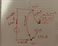
I measured the actual currents right at the supply/GND pins.
+5 V: 30.0 mA at -2 mA output current. 25.9 mA at -4 mA output current. 34.3 mA at zero output current.
-5 V: 39.2 mA fixed
-15 V: 26.45 mA fixed
AGND: 1.93 mA fixed
DGND: 29.55 mA fixed
This is excellent work.
For 5V we see 8mA between zero and full scale, with some error for base currents of bit switches. So this follows published design details of the chip and logical conclusions.
For -5V we obviously only feed CML.
I wonder where audio current flows. It shows only up in +5V, but if we close the loop to AGDN (or DGND) we should see variable current with different codes.
Does the Audio current flow into DGND or AGND?
We have up to ~35mA peak flowing in +5V and into DGND.
We have 39.2mA fixed flow out of -5V (or -39.2mA flow into).
We also have 26.45mA flow out of -15V. So 65.65mA totally flow from AGND & DGND towards -5/-15V.
An average of 30mA flows from +5V into DGND/AGND.
This leaves 35.65mA flowing in the grounds.
We have 29.55mA in DGND leaving 6.1mA to reconcile.
We have 1.93mA reported in AGND reported. Leaving 4.17mA to reconcile. Could this be the two channels ~2mA?
Do they flow into AGND?
I think we have all currents accounted for, just where the current from AOL/AOR returns in unclear, they are left as an irreconcilable 4.17mA amount given the reported numbers.
Still, we have a few conclusions.
First conclusion, AGND is NOT a supply pin, but mostly a "reference". The current for the DEM logic comes from DGND.
Second conclusion, we cannot really separate AGND and DGND.
Third, we are back to a "zener chain" as "optimum" supply.
Thor
Last edited:
I get a 0.13mA? Digital input should be considered?I measured the actual currents right at the supply/GND pins.
+5 V: 30.0 mA at -2 mA output current. 25.9 mA at -4 mA output current. 34.3 mA at zero output current.
-5 V: 39.2 mA fixed
-15 V: 26.45 mA fixed
AGND: 1.93 mA fixed
DGND: 29.55 mA fixed
I double checked the AGND current.
Attachments
Your drawing is much more eye candy.I think this is correct (+/- 1 or 2 mA).
Audio corrent flows from +5V and Iout (L, R) to -15 V. Their sum in the analog path is constant.Does the Audio current flow into DGND or AGND?
I think the +5 V should be well filtered, because the current draw is some fixed value (34.3 mA) minus the (L, R) output current (0 to 8 mA) so it is heavily changing.
The current flowing into -15 V (cca. 26.5 mA) is constant, it is easier to filter it. And there are some current generators at the bit switches IIRC, so it further relaxes the filter requirement here.
....
It may be simpler to use "stopped clock", than to use in effect a FIFO type structure that runs the output at a much lower clock. In discrete logic doing so may simplify design.
My own consideration was to re-design the IIS-2-SIM converter (assumed IIS BCK = 64X FS) to use two sets of 16 Bit Shift registers (74XX16374) to extract the 16 Bit of audio at Fbck into 16 bits parallel (likely stopped clock operation there) and have the output set of 16 Bit Shift registers operate as Parallel to Serial conversion from the 16 Parallel bit running on a BCK of 16 X FS.
With VHC/LCX/AUC logic we have ages of time to transfer the new data in a full BCK clock cycle (likely use negative going BCK edge)
Actually my goal is to fully understand what is going on and to think through all consequences of what goes on to then apply this understanding to design.
Thor
So it's very clear twice for me now it should be took as you said before the Sim mode (when it is still 64 xFs and not x32 AFter the Sim mode).
Off topic, my actual seteup sounds good, but it doesn't stock (good but not my expectation) so a big work on power supplies, regs and passive parts was made, untill each decoupling pins of the TDA1541A with some odds find about gnd decoupling dependantcies between the 3 decoupling rails when a caps multiplier reg are used in relation to the main smoothing cap and its ESR.
I partially gave a mod since 2016 on Audialonline (P Rogic) and keeping some things for myself.
In the IanCanada front end I have that sounded a littlle sterile in my setup which doesn't help (aluminium drivers from 90 Hz acousticaly to 20 K Hz) the front end sounded a little cold, cold in a way it was no accurate or the opposite of warming coloration.
It is async usb with NDK crystals then FiFo-ed, then Reclocked with Crystek top of the line crytals then simultanous mode slaved from the Masterclock, then an AYA board via uf-l plugs all the ways (iso impedance from the Masterclock to the TDA1541A x4 inputs pins (sim mode).
No matter it is I2S or Sim mode, if you do not take care of decoupling and powers supplies it can sounds not good wheiter I2S or Sim mode. I think I learn nothing to folk than know that chip well.
Ultimatly, it sounds very not the same if you use TDA1541A from 89 or from Taiwann 98, whatever the sortting out grade (crowns)
Last edited:
It's above my head, but is the attenuator circuitry making not this slew rate things low enough already ?
Well, we analysed the likely input circuit (TTL to PECL converter is my guess) and this circuit will throw noise related to transition edges into the Substrate, UNLESS the edges are slow enough to not cause large current flow. So slew rate limiting or bandwidth limiting achieves that.
The attenuation has a different purpose.
Our TTL 2 PECL converter likes to see ~ 0.8V ... 2.4V Voltage swing. More than that overdrives the PECL part. This does not cause saturation, but may throw "edge" related noise into +5V or DGND and will take longer to flip polarity as quickly.
So limiting the input swing avoids that second noise source and avoids the NPN Differential Amp that forms the core of PECL "sticking" if driven too far top the rail, which may increase jitter.
It is possible to make attenuators with an impedance that uses the input capacitance of the TDA1541 itself to limit slew rate.
This is in my view a VERY ELEGANT way to do it, but technically questionable, as it relies on a non-guaranteed parameter only indicated under "typical performance" and that we know is actually input signal variable. It should be possible to tune this nicely, but it may not work as expected out of the box.
I remember Thorsten few post ago saying stop clock could be a so-so idea ?!
Stopped clock will not have any benefit in a DAC if there is no material feedthrough from BCK to output.
The TDA1541 specifically seems to have a mechanism that does exactly this.
In this case stopped clock reduces the interference to a fraction of one sample.
Also, as stopped clock has a higher BCK frequency than necessary, the higher frequency with silent periods may filter out easier on the analogue side than a slower continuous clock.
Of course, the problem is not the clock, but the feedthrough and for the TDA1541 we have a solution by which to reduce the feed-through dramatically.
From here:
https://www.mvaudiolabs.com/digital/tda1541-digital-input-attenuation/
To me stopped clock operation of a DAC Chip is a bad idea because it forces higher clock speeds.
I do wonder about slewing and glitches more about the current output of the DAC to be tamed before the first input pin of teh I/V circuitry. But Thorsten Loesch circuitry in his explanation seems to focus on that too!
Cause and effect.
Cause is the combination of the input circuits with fast edges, especially from modern CMOS IC's.
Effect is BCK, Data and WCK ripple on the analogue out.
Second cause is the DEM switching which has short glitches (all switches open) at each switching seen on the DEM Filter pins (essentially a single positive going pulse of 5...20nS.
If they are not filtered they appear on the outputs.
Whatever is left on the analogue output (and there will be always be something) after we deal with all we can still needs addressing.
So we get RF style decoupling for PSU Pin's, DEM Filter Pin's and Output Pin's, essentially all locations on the IC where these glitches can "escape".
We still need to consider the lower frequencies, unless we run circuits that allow us to combine the RF and Audio signal decoupling.
Thor
Thanks a lotI built a standard series regulator for +/- 15V and +/- 5V. These regulators have a common star GND. The AGND and DGND are independently connected to this common star GND. The measurements were taken by disconnecting the +5V, measure the current flowing into pin 28, then doing the same with pin 26 (-5 V) and pin 15 (-15 V). Then I disconnected AGND (pin 5), measured the current, and did the same with DGND (pin 14). This way the current flowing in or out each pin was measured independently. See the jumpers at my picture of the test setup.
very useful infos
Yes, I was going to try balanced. Thanks for the interesting note about what John said regarding jitter.Hi,
Why ? You want balanced or needs higher current output ?
I remember John measured than the too much intrinsec jitter and noise inside the TDA1541A were not favoured a symetric or multiple TDA1541A on board. (And most of what he has were old Taiwan made)
I can add it is also from a pcb layout development an even worse idea....
Remind me when conversion starting for already loaded data, LE rising edge?
There is no "conversion".
All that happens is that the output bit switches are updated to the new state.
What exactly drives that we do not 100% know without a full logic equivalent internal schematic.
We assume it's the LE edge, but it actually may be a BCK edge.
Not sure if @lcsaszar is set up to measure this for IIS & SIM input. A zero to full scale pulse should do it.
Thor
- Home
- Source & Line
- Digital Line Level
- Building the ultimate NOS DAC using TDA1541A