Hi Sven257,
It turned out that the DEM circuit wasn't causing the problem.
The problem is that when digital audio sources are optimised, the “digital” signature gradually gets unmasked and reveals all “digital” nastyness.
Just compare vinyl and studio tape with digital audio sources and the problem becomes clear.
Common fix to this problem is adding a specific distortion spectrum to mask this “digital” signature. This can be done by throwing in some tubes and / or output transfomers. But this masking also masks subtle details in the sound.
So I arrived at a dead end with the TDA1541A project and abandoned it for a while.
As the SD1-player DAC was further optimised, similar issues with “digital” signature showed up.
Recently I was testing yet another circuit for the SD1-player, but this circuit had an unexpected side effect. It seemed to simply remove this “digital” signature while retaining low distortion. This circuit received the nickname “reactor” because of the complex operations it performs in the analogue domain.
This reactor circuit was then tested with the TDA1541A and is the reason I picked up the TDA1541A project again.
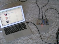
Well picking up is an understatement, a euro card size TDA1541A asynchronous USB DAC prototype with reactor circuit is already up and running (attached picture).
I'm happy to see that you have picked up the TDA1541 DAC project again...
Does that mean you have some new ideas/solutions to deal with the pesky 'DEM circuit’??
It turned out that the DEM circuit wasn't causing the problem.
The problem is that when digital audio sources are optimised, the “digital” signature gradually gets unmasked and reveals all “digital” nastyness.
Just compare vinyl and studio tape with digital audio sources and the problem becomes clear.
Common fix to this problem is adding a specific distortion spectrum to mask this “digital” signature. This can be done by throwing in some tubes and / or output transfomers. But this masking also masks subtle details in the sound.
So I arrived at a dead end with the TDA1541A project and abandoned it for a while.
As the SD1-player DAC was further optimised, similar issues with “digital” signature showed up.
Recently I was testing yet another circuit for the SD1-player, but this circuit had an unexpected side effect. It seemed to simply remove this “digital” signature while retaining low distortion. This circuit received the nickname “reactor” because of the complex operations it performs in the analogue domain.
This reactor circuit was then tested with the TDA1541A and is the reason I picked up the TDA1541A project again.
Well picking up is an understatement, a euro card size TDA1541A asynchronous USB DAC prototype with reactor circuit is already up and running (attached picture).
Attachments
...
Well picking up is an understatement, a euro card size TDA1541A asynchronous USB DAC prototype with reactor circuit is already up and running (attached picture).
😀 Drool!
That is exactly what I've been looking for! Almost all (99.99%) of my music is regular CD ripped to .flac so I don't need 96k, ...192k ... 384k! 😱
I've been looking for a good USB solution and have been playing with USB to I2S converters and multibit DACs (1545/1387 and 1541)
Keep up the good work!
Last edited:
reactor circuit schematic
Hi ECDesigns,
I enjoyed your DAC optimization proces so far and enjoy the audible results. Nice work and thanks for sharing.
Is a reactor circuit schematic availeble for publication?
Best regards,
Henk
Hi ECDesigns,
I enjoyed your DAC optimization proces so far and enjoy the audible results. Nice work and thanks for sharing.
Is a reactor circuit schematic availeble for publication?
Best regards,
Henk

Hi all,
if anyone was interested in the custom Laptech crystal
http://www.diyaudio.com/forums/grou...hronous-i2s-s-pdif-fifo-kit-group-buy-70.html
please add your name in the wish list at
http://www.diyaudio.com/forums/digital-line-level/203511-any-good-tda1541a-dac-kit-96.html
The minimum orderable quantity from Laptech is 5 pcs for each frequency.
When that quantity will be reached I ask Laptech for a quote.
Andrea
Hi,
j have just finished to configure my 2 X TDA 1541 in // with Dvb project pcb, and as j have the old board without output stage, j am using the jfet IV from spencer
http://www.fetaudio.com/wp-content/uploads/2009/10/Jfet-IV-Regulator-4.pdf.
It's working, but what do you think about this solution.
With R4 j have 1.5K for two TDA if j use 1K it is not possible to reach 10V as suggest on the schematic (max8V). Is there a way to adapt better for the 2 TDA 1541A or j have to find an other schematic. J had the idea to add a resistor (5K) from ouput to + 20V Rail in order to have 4ma
Thanks for your help
Hi COX77,
I personally wouldn’t use the I/V converter design you posted, it’s over complicated, instable and ineffective.
When you -have- to parallel DAC chips, it's much better to use dual mono configuration:
TDA1541A # 1 outputs L/L (both, L & R outputs connected in parallel).
TDA1541A # 2 outputs R/R (both, L & R outputs connected in parallel).
This requires an I2S splitter circuit. Simplest version (with BCK frequency limitation to approx. 3 MHz) could be constructed from one CD4517 and one 74HC157 chip.
Suitable I/V converter circuit that outputs 10Vpp (1K25 I/V resistor) and runs from TDA1541A +5V, -5V, and -15V could be constructed with only 5 parts, no matched components and no adjustments.
j have just finished to configure my 2 X TDA 1541 in // with Dvb project pcb, and as j have the old board without output stage, j am using the jfet IV from spencer
I personally wouldn’t use the I/V converter design you posted, it’s over complicated, instable and ineffective.
When you -have- to parallel DAC chips, it's much better to use dual mono configuration:
TDA1541A # 1 outputs L/L (both, L & R outputs connected in parallel).
TDA1541A # 2 outputs R/R (both, L & R outputs connected in parallel).
This requires an I2S splitter circuit. Simplest version (with BCK frequency limitation to approx. 3 MHz) could be constructed from one CD4517 and one 74HC157 chip.
Suitable I/V converter circuit that outputs 10Vpp (1K25 I/V resistor) and runs from TDA1541A +5V, -5V, and -15V could be constructed with only 5 parts, no matched components and no adjustments.
Thank you for your help
Do you think about this circuit
Balanced DAC I2S interface project - Audial online topic
As j need a buffer after the WM 8804 module and the i2S attenuator a put the buffer before or after thus i2S split
J haven not understand your suggestion circuit for the output stage
Philippe
Do you think about this circuit
Balanced DAC I2S interface project - Audial online topic
As j need a buffer after the WM 8804 module and the i2S attenuator a put the buffer before or after thus i2S split
J haven not understand your suggestion circuit for the output stage
Philippe
This requires an I2S splitter circuit. Simplest version (with BCK frequency limitation to approx. 3 MHz) could be constructed from one CD4517 and one 74HC157 chip.
Suitable I/V converter circuit that outputs 10Vpp (1K25 I/V resistor) and runs from TDA1541A +5V, -5V, and -15V could be constructed with only 5 parts, no matched components and no adjustments.
Could you post a schema of the i2s splitter? I would like to use it on 1543
Last edited:
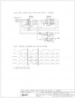
I2S dual mono splitter
Hi marconi118,
I attached the schematic of the I2S dual mono splitter.
It already contains DATA and WS buffers / level translators so this circuit works with digital audio sources with 3V3 and 5V signal levels.
The circuit works with both, TDA1543 and TDA1541A
The outputs are L/L and R/R and both L and R outputs of one DAC chips are paralleled as in the schematic.
The timing diagram illustrates how the circuit works. The CD4517 provides required delays of 32, 64, and 96 bit clock periods.
The 74HC157 (quad, 2 input multiplexer) is used for buffering & level conversion and for selecting the correct delay depending on WS signal level. All multiplexters change state with the WS signal that enters pin 1.
This circuit could be converted to a L/-L and R/-R splitter by adding two inverters. One at pin 10 of U1 and one at pin 13 of U1. One could use 74HC04 for this.
Hi marconi118,
Could you post a schema of the i2s splitter? I would like to use it on 1543
I attached the schematic of the I2S dual mono splitter.
It already contains DATA and WS buffers / level translators so this circuit works with digital audio sources with 3V3 and 5V signal levels.
The circuit works with both, TDA1543 and TDA1541A
The outputs are L/L and R/R and both L and R outputs of one DAC chips are paralleled as in the schematic.
The timing diagram illustrates how the circuit works. The CD4517 provides required delays of 32, 64, and 96 bit clock periods.
The 74HC157 (quad, 2 input multiplexer) is used for buffering & level conversion and for selecting the correct delay depending on WS signal level. All multiplexters change state with the WS signal that enters pin 1.
This circuit could be converted to a L/-L and R/-R splitter by adding two inverters. One at pin 10 of U1 and one at pin 13 of U1. One could use 74HC04 for this.
Attachments
Hi John,
Pls excuse my ignorance. What advantage does dual mono
have over parallel dac ? We're still summing the output of both
dac together but in a different manner .
Thks
Pls excuse my ignorance. What advantage does dual mono
have over parallel dac ? We're still summing the output of both
dac together but in a different manner .
Thks
Thank you very much for the schématic.
if j add the inverter j can use the TDA1541 A in simultaneous mode ?
I
if j add the inverter j can use the TDA1541 A in simultaneous mode ?
I
Hi Jaffrie,
- Good matching and thermal tracking of both paralleled DAC chips (both DAC sections are located on the same chip).
- Noise / jitter spectrum only relates to one channel that is being processed by that chip instead of a mix from L and R channel.
- Greatly reduced crosstalk between L and R channels. Crosstalk significantly increases when paralleling multiple stereo DAC chips.
- Tolerances in full scale current between L and R channel on the same chip that are related to chip design are cancelled as the same tolerances now occur for both channels.
DAC chips have different propagation delay between BCK / LE signal change and output latching. This time can be measured with a frequency counter.
This means that when paralleling DAC chips that have different propagation delay, the outputs won’t latch exactly simultaneously but rather one after the other. Propagation delay can also change with thermal drift (not constant).
This can introduce significant jitter. Jitter amplitude and spectrum change with amount of paralleled DAC chips and the thermal drift in all DAC chips ensures that sound quality isn’t constant.
Matched DAC sections (located on the same chip) with excellent thermal tracking will minimise this issue with propagation delay (changes). This again can be measured with a frequency counter.
One has to trigger the counter with the BCK / LE signal and stop counting as soon as a new sample is latched at the output. 0dB Square wave test signal can be used for this. The measurement shows tolerances in propagation delay and change of propagation delay as a result of chip temperature changes.
When stacking TDA1543 chips, the chips in the center of the stack get hotter, so propagation delay of these chips will already be quite different from the propagation delay of chips located at the top or bottom of the stack. This, together with tolerances in propagation delay ensures high jitter levels due to non-simultaneous latching.
Similar issues also occur with non-matched delta sigma DAC chips that are not thermally coupled.
So in general it is not a good idea to simply parallel randomly selected unmatched DAC chips as this will almost certainly lead to degraded sound quality compared to a single DAC chip.
Dual mono configuration can be useful to double full scale output current (better switching characteristics, lower I/V resistor value for same output signal amplitude). Since the full scale current of the TDA1543 for example is rather low (2.3 … 2.5mA) and on-chip crosstalk is rather high, it is a good idea to use these chips in dual mono mode.
Pls excuse my ignorance. What advantage does dual mono
have over parallel dac ? We're still summing the output of both
dac together but in a different manner .
- Good matching and thermal tracking of both paralleled DAC chips (both DAC sections are located on the same chip).
- Noise / jitter spectrum only relates to one channel that is being processed by that chip instead of a mix from L and R channel.
- Greatly reduced crosstalk between L and R channels. Crosstalk significantly increases when paralleling multiple stereo DAC chips.
- Tolerances in full scale current between L and R channel on the same chip that are related to chip design are cancelled as the same tolerances now occur for both channels.
DAC chips have different propagation delay between BCK / LE signal change and output latching. This time can be measured with a frequency counter.
This means that when paralleling DAC chips that have different propagation delay, the outputs won’t latch exactly simultaneously but rather one after the other. Propagation delay can also change with thermal drift (not constant).
This can introduce significant jitter. Jitter amplitude and spectrum change with amount of paralleled DAC chips and the thermal drift in all DAC chips ensures that sound quality isn’t constant.
Matched DAC sections (located on the same chip) with excellent thermal tracking will minimise this issue with propagation delay (changes). This again can be measured with a frequency counter.
One has to trigger the counter with the BCK / LE signal and stop counting as soon as a new sample is latched at the output. 0dB Square wave test signal can be used for this. The measurement shows tolerances in propagation delay and change of propagation delay as a result of chip temperature changes.
When stacking TDA1543 chips, the chips in the center of the stack get hotter, so propagation delay of these chips will already be quite different from the propagation delay of chips located at the top or bottom of the stack. This, together with tolerances in propagation delay ensures high jitter levels due to non-simultaneous latching.
Similar issues also occur with non-matched delta sigma DAC chips that are not thermally coupled.
So in general it is not a good idea to simply parallel randomly selected unmatched DAC chips as this will almost certainly lead to degraded sound quality compared to a single DAC chip.
Dual mono configuration can be useful to double full scale output current (better switching characteristics, lower I/V resistor value for same output signal amplitude). Since the full scale current of the TDA1543 for example is rather low (2.3 … 2.5mA) and on-chip crosstalk is rather high, it is a good idea to use these chips in dual mono mode.
Hi John,
Thank you so kindly for the tutorial. Never occur to me
in this manner but is it not a catch 22 situation whereby using
a I2s splitter, inverter it might corrupt the signal prior. Would
it not end up solving one problem n introducing another?
Thank again
Thank you so kindly for the tutorial. Never occur to me
in this manner but is it not a catch 22 situation whereby using
a I2s splitter, inverter it might corrupt the signal prior. Would
it not end up solving one problem n introducing another?
Thank again
Hi John,
Great news regarding your "reactor" circuit, that removes the "digital" signature while retaining low distortion... That got you to pick up the TDA1541A project again...
Regarding the I2S splitter dual mono TDA1541A circuit with the benefits you mention, are you maybe going that rout??
Peter
Great news regarding your "reactor" circuit, that removes the "digital" signature while retaining low distortion... That got you to pick up the TDA1541A project again...
Regarding the I2S splitter dual mono TDA1541A circuit with the benefits you mention, are you maybe going that rout??
Peter
Hi Jaffrie,
I tested a TDA1543 single, two paralleled and dual mono configuration side by side. The dual mono configuration provides best perceived sound that comes closest to that of an optimised TDA1541A circuit. So the I2S splitter clearly offers advantages here.
The signal is not corrupted, bit perfect L / L or R / R data is latched into the DAC chip. The circuit only delays I2S signals so the data can be aligned (diagram added to the I2S splitter schematic). The 74HC157 selects a specific delay time depending on WS signal status.
I have to add that I always test with the reactor circuit installed now.
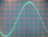
I attached an oscillogram of the reactor circuit output signal of an early prototype. The reactor circuit basically super imposes an analogue sawtooth signal to the zero order output signal of the DAC chip. Polarity and amplitude change with sample polarity and value. The sawtooth signal contains even order harmonics. In contrast with the zero order hold signal, the reactor output signal keeps changing during sample hold time (ramping up or ramping down).
Thank you so kindly for the tutorial. Never occur to me
in this manner but is it not a catch 22 situation whereby using
a I2s splitter, inverter it might corrupt the signal prior. Would
it not end up solving one problem n introducing another?
I tested a TDA1543 single, two paralleled and dual mono configuration side by side. The dual mono configuration provides best perceived sound that comes closest to that of an optimised TDA1541A circuit. So the I2S splitter clearly offers advantages here.
The signal is not corrupted, bit perfect L / L or R / R data is latched into the DAC chip. The circuit only delays I2S signals so the data can be aligned (diagram added to the I2S splitter schematic). The 74HC157 selects a specific delay time depending on WS signal status.
I have to add that I always test with the reactor circuit installed now.
I attached an oscillogram of the reactor circuit output signal of an early prototype. The reactor circuit basically super imposes an analogue sawtooth signal to the zero order output signal of the DAC chip. Polarity and amplitude change with sample polarity and value. The sawtooth signal contains even order harmonics. In contrast with the zero order hold signal, the reactor output signal keeps changing during sample hold time (ramping up or ramping down).
Attachments
Hi Sven257,
The dual mono circuit was tested with the TDA1543 in order to increase full scale current. This in turn was required to increase output signal amplitude while maintaining same I/V resistor value and improve bit switching characteristics.
The idea was using this circuit in a new version of the SD1-player.
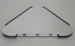
However, we finally decided to use the TDA1541A instead.
Both, UD2 DAC and the new SD2-player will be based on the TDA1541A and the reactor circuit.
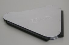
Both projects will fit in a similar 12mm high housing (attached pictures show the already completed UD2 DAC).
Regarding the I2S splitter dual mono TDA1541A circuit with the benefits you mention, are you maybe going that rout??
The dual mono circuit was tested with the TDA1543 in order to increase full scale current. This in turn was required to increase output signal amplitude while maintaining same I/V resistor value and improve bit switching characteristics.
The idea was using this circuit in a new version of the SD1-player.
However, we finally decided to use the TDA1541A instead.
That got you to pick up the TDA1541A project again…
Both, UD2 DAC and the new SD2-player will be based on the TDA1541A and the reactor circuit.
Both projects will fit in a similar 12mm high housing (attached pictures show the already completed UD2 DAC).
Attachments
I will use the splitter to avoid using the left channel of the 1543
use only the right channel on each of the 2 1543 for R / L output
it seems according some forums that the left channel has higher distortion
and less resolution than the right channel
Is this true?
DIYHiFi.org • View topic - Pushing the limits of TDA1543 NOS DAC
use only the right channel on each of the 2 1543 for R / L output
it seems according some forums that the left channel has higher distortion
and less resolution than the right channel
Is this true?
DIYHiFi.org • View topic - Pushing the limits of TDA1543 NOS DAC
Hi All,
I have been reading this thread on and off.
This is my first post.
In one of John's posts, 8) "Use a suitable low jitter external DEM clock instead of the on-chip DEM oscillator that produces very high jitter.--------------The latest circuit I have used is a simple diode-resistor injector that is fed with 44.1KHz WS signal"
I would like to implement the circuit in my DAC.
Please tell me where I can get the schematic. BTW, I have implemented the I2S atteunation circuit.
Thanks to all
Goh
- Home
- Source & Line
- Digital Line Level
- Building the ultimate NOS DAC using TDA1541A