These are custom parts, both OCXO and crystal are 11.2896MHz.Nice find! May I ask what the price of these babies is? Also, is it spec'ed at -130db or did you measure? I can't find the datasheet on the Laptech page (don't know which one it is....
-130dBc@10Hz for the OCXO was measured form the manufacturer before shipment, I published the measurement document in Ian's FIFO buffer thread, if i remember correct. The OCXO is very expensive, around 300 GBP without VAT and shipping.
You cannot find the Laptech sheet because it's a custom part; less than 10 ohm ESR and Q greater than 150K was measured by the manufacturer. It costs around 35 CAD excluding VAT and shipping for 5 pcs.
I'm working on a low phase noise oscillator using the Laptech crystal.
About the BCK, I meant to feed it directly from the XO, without any reclocker, so 2.8224 or 5.6448MHz (32 or 64 bit words in NOS mode) for the TDA1541A, then a frequency multiplier for the source clock if it need higher frequency.As long as BCK is reclocked, it's probably indeed better to feed the cleanest clock signal to the reclocker and the multiplied clock signal to the source. The picture you show is of a 11mhz crystal though 😕
Thanks. It is a clear picture you paint.
Do I infer too much if I state, using you words:
albert 🙂
Do I infer too much if I state, using you words:
"With conventional applications with low time resolution it has no advantages to use a TDA1543" --> with state of the art applications with high time resolution it has many advantages to use a TDA1543.
albert 🙂
Hi triode_al,
If only I could simply share perceived sound quality of various prototypes. But even modern technology fails to offer this possibility over the internet.
[--]
TDA1541A is based on current mode logic too, but the on-chip circuits are more complex (DEM circuit), so DAC chip jitter contribution is likely to be higher. The advantage of the DEM logic is increased bit accuracy without (LASER) trimming, but without matching time resolution (that is degraded by this same DEM circuit), the DEM circuit has little added value.
These DAC chip properties only start to have a big impact when external circuits are approaching perfection (extreme low jitter, extreme high time resolution). With conventional applications with low time resolution it has no advantages to use a TDA1543.
@ John
For a quick verification if everything is correct! 🙄
An externally hosted image should be here but it was not working when we last tested it.
Doei,
Oliver

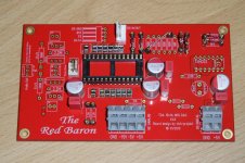
Hi John,
i had integrated all changes above on my Red Baron test board. The 3.3V comes from one of my +5V SSLV Shunt modules (modified). It worked great! 😛
Now the only question is, should we attenuate the BCK to your regarded 800mVpp with perhaps some TX2575 bulk foil resistors? 🙄
Best regards,
Oliver
Attachments
Hi John,
[--] , should we attenuate the BCK to your regarded 800mVpp with resistors? 🙄
Best regards,
Oliver
I just had a look at the TDA1543 datasheet, as it has the similar input schema, and there also BCK has this similar input configuration - no resistors in the signal.
just my 2 ¢
albert
Is it necessary to add 2mA to TDA1541 outputs while I\U is provided by OpAmp? (Stock variant like NE5532\LM833) Or this is only for resistor I\U?
According to TDA1541 datasheet this is not required.
But if I/U is provided by opa-amp, accompaniment of 2 mA on output 1541 reduces the current through feedback resistor. This reduces the constant voltage on a opa-amp output (in ideal up to zero).
From others experience, which has more sonic benefit:
a) Provide the 2mA bias to the TDA1541A output from a constant current source, and eliminate the coupling capacitor from the output of the opamp, or
b) Let it flow through the opamp feedback resistor, and use a good quality output coupling capacitor?
a) Provide the 2mA bias to the TDA1541A output from a constant current source, and eliminate the coupling capacitor from the output of the opamp, or
b) Let it flow through the opamp feedback resistor, and use a good quality output coupling capacitor?
a) Provide the 2mA bias to the TDA1541A output from a constant current source, and eliminate the coupling capacitor from the output of the opamp, or
b) Let it flow through the opamp feedback resistor, and use a good quality output coupling capacitor?
Put or not to put the output capacitor - this is separate question. But I prefer variant 1.
just want to say that I will get my hand on one of the sd1 player real soon, will report back my impression. The comparison will be against a buffalo dac!
with state of the art applications with high time resolution it has many advantages to use a TDA1543
If this is true, what about TDA1545?
Should have an even better sound than 1543 without the DEM clock problems?
can we use the same mk7 output stage on a TDA1545? what about the -15v bias to the mosfet?
If this is true, what about TDA1545?
Should have an even better sound than 1543 without the DEM clock problems?
can we use the same mk7 output stage on a TDA1545? what about the -15v bias to the mosfet?
If this is true, what about TDA1545?
TDA1545 and TDA1543 vastly worse, than TDA1541(A). For TDA1545 THD is equal -88 dB at level of the signal 0 dB (-95 dB for TDA1541) and -35 dB at level of the signal -60 dB (-42 dB for TDA1541).
and comparing tda1543 to tda1545?
Ecdesign mentioned earlier that 1543 is better than 1541 for SD player, less internal jiiter
Ecdesign mentioned earlier that 1543 is better than 1541 for SD player, less internal jiiter
and comparing tda1543 to tda1545?
THD for TDA1543: -75 dB and -30 dB for signal level 0 dB and -60 dB accordingly. Else worse, than at TDA1545.
Ecdesign mentioned earlier that 1543 is better than 1541 for SD player, less internal jiiter
I can't agree with this opinion. It is deeply wrongly.
If this is true, what about TDA1545?
Should have an even better sound than 1543 without the DEM clock problems?
I've found that TDA1545A does sound better than 1543 but only when the output is carefully filtered to reduce the glitching. Being a CMOS chip it generates a substantial quantity of switching noise on its PSU. If the impact of this HF noise on the following circuitry isn't minimized, it sounds more gritty than 1543 despite posting better specs.
Hi marconi118,
The SDV1-player was specifically designed to obtain highest possible time resolution with currently available (and affordable) parts. Feedback from audiophiles suggests that this is a -highly- desirable feature in digital audio sources.
Note that just using a TDA1543 in an application is meaningless without providing the environment required for obtaining highest possible time resolution.
TDA1545 is based on noisy CMOS logic (4mA supply current) and the continuous calibration causes similar problems like with DEM. So it is unusable for obtaining high time resolution.
The reason why I am no longer using ultra high speed CMOS circuits for clock, clock distribution, and DAC chip is that these have approx. 12.5 times higher jitter contribution compared to CML / ECL.
Typical jitter contribution of an ultra high speed CMOS (275 MHz): 2.5ps
Typical jitter contribution of CML / ECL (4 GHz): 0.2ps
The reduction of approx. 2.5ps to 0.2 ps is -very- clearly audible with NOS that is -least- sensitive to jitter.
The jitter spectrum is alo of greatest importance for perceived sound quality. So when jitter amplitude has reached its practical limits, further improvements can be made by tuning the residual jitter spectrum.
with state of the art applications with high time resolution it has many advantages to use a TDA1543
If this is true, what about TDA1545?
The SDV1-player was specifically designed to obtain highest possible time resolution with currently available (and affordable) parts. Feedback from audiophiles suggests that this is a -highly- desirable feature in digital audio sources.
Note that just using a TDA1543 in an application is meaningless without providing the environment required for obtaining highest possible time resolution.
TDA1545 is based on noisy CMOS logic (4mA supply current) and the continuous calibration causes similar problems like with DEM. So it is unusable for obtaining high time resolution.
The reason why I am no longer using ultra high speed CMOS circuits for clock, clock distribution, and DAC chip is that these have approx. 12.5 times higher jitter contribution compared to CML / ECL.
Typical jitter contribution of an ultra high speed CMOS (275 MHz): 2.5ps
Typical jitter contribution of CML / ECL (4 GHz): 0.2ps
The reduction of approx. 2.5ps to 0.2 ps is -very- clearly audible with NOS that is -least- sensitive to jitter.
The jitter spectrum is alo of greatest importance for perceived sound quality. So when jitter amplitude has reached its practical limits, further improvements can be made by tuning the residual jitter spectrum.
Afaik the main jitter bottleneck for ECLs was the ECL-TTL conversion which was worse than going with TTL all the way.
So when jitter amplitude has reached its practical limits, further improvements can be made by tuning the residual jitter spectrum.
Hi, -ecdesigns-
How you offer to adjust the jitter spectrum?
Hi s3tup,
True, one ECL to TTL translator would contribute approx. 2.5ps of jitter. This would equal the jitter contribution of a single ultra high speed CMOS gate.
But why convert ECL to TTL when using TDA154x DAC chips that are already based on Current Mode Logic with typical 400mVpp signal swing?
ECL can drive TDA154x chips perfectly while providing very low jitter contribution.
Afaik the main jitter bottleneck for ECLs was the ECL-TTL conversion which was worse than going with TTL all the way.
True, one ECL to TTL translator would contribute approx. 2.5ps of jitter. This would equal the jitter contribution of a single ultra high speed CMOS gate.
But why convert ECL to TTL when using TDA154x DAC chips that are already based on Current Mode Logic with typical 400mVpp signal swing?
ECL can drive TDA154x chips perfectly while providing very low jitter contribution.
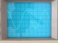
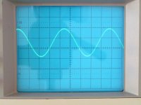
Hi SSerg,
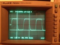
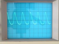
I use an electronic tuning fork. Phase noise spectrum tuning is mainly obtained by tuning the properties of the active single transistor drive circuit.
First oscillogram shows the drive signal (input node, 0.5V/div, 11.289 MHz).
Second oscillogram shows the signal on the primary node (1V/div, 11.289 MHz).
Third oscillogram shows the signal on the secondary node (1V/div, 11.289 MHz).
All 3 nodes are "isolated" for all frequencies but the fundamental (11.289 MHz). This prevents cross-pollution between connected circuits.
The microcontroller is connected to the primary node using a low pass fliter / attenuator
The PECL divider is connected to the secondary node.
PECL divider circuit outputs 800mVpp BCK signal with exactly 1.1V DC bias.
How you offer to adjust the jitter spectrum?
I use an electronic tuning fork. Phase noise spectrum tuning is mainly obtained by tuning the properties of the active single transistor drive circuit.
First oscillogram shows the drive signal (input node, 0.5V/div, 11.289 MHz).
Second oscillogram shows the signal on the primary node (1V/div, 11.289 MHz).
Third oscillogram shows the signal on the secondary node (1V/div, 11.289 MHz).
All 3 nodes are "isolated" for all frequencies but the fundamental (11.289 MHz). This prevents cross-pollution between connected circuits.
The microcontroller is connected to the primary node using a low pass fliter / attenuator
The PECL divider is connected to the secondary node.
PECL divider circuit outputs 800mVpp BCK signal with exactly 1.1V DC bias.
Attachments
Last edited:
- Home
- Source & Line
- Digital Line Level
- Building the ultimate NOS DAC using TDA1541A