Hi John
In your MK6 dac schematic, why do you put -15 volt at R18 and R19 ?
I can't find the 74AU1G74 here arround, is there some more easy to find, like any low jitter 74HCxx, 74Fxx or 74ACxx, that I can use ?
Thanx
Paul
In your MK6 dac schematic, why do you put -15 volt at R18 and R19 ?
I can't find the 74AU1G74 here arround, is there some more easy to find, like any low jitter 74HCxx, 74Fxx or 74ACxx, that I can use ?
Thanx
Paul
Attachments
Last edited:
feeding the dac
with lithium batteries
That works very very good ...only don`t charge wile playing then you hear the distortion again 😛
Done it with a 5A 12V battery but those where nicad

Hi tessier,
These are part of voltage dividers that put variable negative bias voltages on both DEM oscillator inputs in order to synchronize it.
The 2.8224 MHz balanced DEM clock drive signal creates DC voltage swing on each DEM oscillator pin that varies between -12.58 and -12.36V. So it creates a balanced 440mVpp drive signal between pins 16 and 17 with an average negative bias voltage of -12.47V.
This balanced DC-coupled clock signal with -12.47V negative bias is required to synchronize the on-chip DEM oscillator.
TDA1541A uses current steering logic that consists of a CCS and transistor, it only requires low level drive signals of up to 1Vpp. Because of this fast current steering logic, TDA1541A has very low additive jitter. Now jitter at the D/A stage manly depends on external timing signal jitter amplitude.
The 74AU1G74 is the only suitable CMOS D flip-flop I could find. Popular flip-flops like HC, F, and AC series add unacceptable jitter levels. You could also experiment with (P)ECL.
Here is a list with popular audio formats and calculated max. tolerable jitter amplitude (at the D/A stage inside the DAC chip) for given resolution. This is based on the fact that sample timing variation (jitter) is a form of PWM and changes sample value similar to sample amplitude. So the net averaged / filtered sample energy is not only affected by sample amplitude but also by sample duration. Measurements don't show this when displaying signal amplitude only. Jitter is too low to be visible when viewing a 1 KHz test signal.
44.1/16 NOS, 0.1 LSB (15.5 bit resolution), 1 / (44,100 * 1) / (2^16 / (1 / 0.5)) = 173ps.
44.1/16 NOS, 0.1 LSB (15.9 bit resolution), 1 / (44,100 * 1) / (2^16 / (1 / 0.1)) = 34.6ps.
44.1/16 NOS, 0.01 LSB (15.99 bit resolution),1 / (44,100 * 1) / (2^16 / (1 / 0.01)) = 3.46ps.
44.1/16, 8 * oversampling, 0.5 LSB error (15.5 bit resolution), 1 / (44,100 * 8) / (2^16 / (1 / 0.5)) = 21.625ps.
44.1/16, 8 * oversampling, 0.1 LSB error (15.9 bit resolution), 1 / (44,100 * 8) / (2^16 / (1 / 0.1)) = 4.32ps.
44.1/16, 8 * oversampling, 0.01 LSB error (15.99 bit resolution), 1 / (44,100 * 8) / (2^16 / (1 / 0.01)) = 432 femto seconds.
96/24 NOS, 0.5 LSB (23.5 bit resolution), 1 / (96,000 * 1) / (2^24 / (1 / 0.5)) = 310 femto seconds.
96/24 NOS, 0.1 LSB (23.9 bit resolution), 1 / (96,000 * 1) / (2^24 / (1 / 0.1)) = 62 femto seconds.
96/24 NOS, 0.01 LSB (23.99 bit resolution), 1 / (96,000 * 1) / (2^24 / (1 / 0.01)) = 6.2 femtoseconds.
96/24 8 * OS, 0.5 LSB (23.5 bit resolution), 1 / (96,000 * 8) / (2^24 / (1 / 0.5)) = 38.8 femtoseconds.
96/24 8 * OS, 0.1 LSB (23.9 bit resolution), 1 / (96,000 * 8) / (2^24 / (1 / 0.1)) = 7.76 femtoseconds.
96/24 8 * OS, 0.01 LSB (23.99 bit resolution), 1 / (96,000 * 8) / (2^24 / (1 / 0.01)) = 776 attoseconds.
192/24 NOS, 0.5 LSB (23.5 bit resolution), 1 / (96,000 * 1) / (2^24 / (1 / 0.5)) = 155 femtoseconds.
192/24 NOS, 0.1 LSB (23.9 bit resolution), 1 / (96,000 * 1) / (2^24 / (1 / 0.1)) = 31 femtoseconds.
192/24 NOS, 0.01 LSB (23.99 bit resolution), 1 / (96,000 * 1) / (2^24 / (1 / 0.01)) = 3.1 femtoseconds.
192/24 8 * OS, 0.5 LSB (23.5 bit resolution), 1 / (96,000 * 8) / (2^24 / (1 / 0.5)) = 19.4 femtoseconds.
192/24 8 * OS, 0.1 LSB (23.9 bit resolution), 1 / (96,000 * 8) / (2^24 / (1 / 0.1)) = 3.88 femto seconds.
192/24 8 * OS, 0.01 LSB (23.99 bit resolution), 1 / (96,000 * 8) / (2^24 / (1 / 0.01)) = 388 attoseconds.
1000 femtoseconds equal 1 picosecond.
1000 attoseconds equal 1 femtosecond, 1000,000 attoseconds equal 1 picosecond.
Failing to meet above jitter requirements, leads to (substantial) loss of resolution.
Jitter sensitivity rises rapidly with higher sample rates and oversampling.
In your MK6 dac schematic, why do you put -15 volt at R18 and R19 ?
These are part of voltage dividers that put variable negative bias voltages on both DEM oscillator inputs in order to synchronize it.
The 2.8224 MHz balanced DEM clock drive signal creates DC voltage swing on each DEM oscillator pin that varies between -12.58 and -12.36V. So it creates a balanced 440mVpp drive signal between pins 16 and 17 with an average negative bias voltage of -12.47V.
This balanced DC-coupled clock signal with -12.47V negative bias is required to synchronize the on-chip DEM oscillator.
TDA1541A uses current steering logic that consists of a CCS and transistor, it only requires low level drive signals of up to 1Vpp. Because of this fast current steering logic, TDA1541A has very low additive jitter. Now jitter at the D/A stage manly depends on external timing signal jitter amplitude.
I can't find the 74AU1G74 here arround, is there some more easy to find, like any low jitter 74HCxx, 74Fxx or 74ACxx, that I can use ?
The 74AU1G74 is the only suitable CMOS D flip-flop I could find. Popular flip-flops like HC, F, and AC series add unacceptable jitter levels. You could also experiment with (P)ECL.
Here is a list with popular audio formats and calculated max. tolerable jitter amplitude (at the D/A stage inside the DAC chip) for given resolution. This is based on the fact that sample timing variation (jitter) is a form of PWM and changes sample value similar to sample amplitude. So the net averaged / filtered sample energy is not only affected by sample amplitude but also by sample duration. Measurements don't show this when displaying signal amplitude only. Jitter is too low to be visible when viewing a 1 KHz test signal.
44.1/16 NOS, 0.1 LSB (15.5 bit resolution), 1 / (44,100 * 1) / (2^16 / (1 / 0.5)) = 173ps.
44.1/16 NOS, 0.1 LSB (15.9 bit resolution), 1 / (44,100 * 1) / (2^16 / (1 / 0.1)) = 34.6ps.
44.1/16 NOS, 0.01 LSB (15.99 bit resolution),1 / (44,100 * 1) / (2^16 / (1 / 0.01)) = 3.46ps.
44.1/16, 8 * oversampling, 0.5 LSB error (15.5 bit resolution), 1 / (44,100 * 8) / (2^16 / (1 / 0.5)) = 21.625ps.
44.1/16, 8 * oversampling, 0.1 LSB error (15.9 bit resolution), 1 / (44,100 * 8) / (2^16 / (1 / 0.1)) = 4.32ps.
44.1/16, 8 * oversampling, 0.01 LSB error (15.99 bit resolution), 1 / (44,100 * 8) / (2^16 / (1 / 0.01)) = 432 femto seconds.
96/24 NOS, 0.5 LSB (23.5 bit resolution), 1 / (96,000 * 1) / (2^24 / (1 / 0.5)) = 310 femto seconds.
96/24 NOS, 0.1 LSB (23.9 bit resolution), 1 / (96,000 * 1) / (2^24 / (1 / 0.1)) = 62 femto seconds.
96/24 NOS, 0.01 LSB (23.99 bit resolution), 1 / (96,000 * 1) / (2^24 / (1 / 0.01)) = 6.2 femtoseconds.
96/24 8 * OS, 0.5 LSB (23.5 bit resolution), 1 / (96,000 * 8) / (2^24 / (1 / 0.5)) = 38.8 femtoseconds.
96/24 8 * OS, 0.1 LSB (23.9 bit resolution), 1 / (96,000 * 8) / (2^24 / (1 / 0.1)) = 7.76 femtoseconds.
96/24 8 * OS, 0.01 LSB (23.99 bit resolution), 1 / (96,000 * 8) / (2^24 / (1 / 0.01)) = 776 attoseconds.
192/24 NOS, 0.5 LSB (23.5 bit resolution), 1 / (96,000 * 1) / (2^24 / (1 / 0.5)) = 155 femtoseconds.
192/24 NOS, 0.1 LSB (23.9 bit resolution), 1 / (96,000 * 1) / (2^24 / (1 / 0.1)) = 31 femtoseconds.
192/24 NOS, 0.01 LSB (23.99 bit resolution), 1 / (96,000 * 1) / (2^24 / (1 / 0.01)) = 3.1 femtoseconds.
192/24 8 * OS, 0.5 LSB (23.5 bit resolution), 1 / (96,000 * 8) / (2^24 / (1 / 0.5)) = 19.4 femtoseconds.
192/24 8 * OS, 0.1 LSB (23.9 bit resolution), 1 / (96,000 * 8) / (2^24 / (1 / 0.1)) = 3.88 femto seconds.
192/24 8 * OS, 0.01 LSB (23.99 bit resolution), 1 / (96,000 * 8) / (2^24 / (1 / 0.01)) = 388 attoseconds.
1000 femtoseconds equal 1 picosecond.
1000 attoseconds equal 1 femtosecond, 1000,000 attoseconds equal 1 picosecond.
Failing to meet above jitter requirements, leads to (substantial) loss of resolution.
Jitter sensitivity rises rapidly with higher sample rates and oversampling.
about the Circlotron amp, is it possible to use 22V transformers instead of 18v ones?
Any resistor value to modify?
Any resistor value to modify?
Hi marconi118,
Yes.
If you plan to increase output power, resistor values need to be recalculated, higher gain MOSFETs are required for the input / driver stage, and power supply voltages for the input / driver stage need to be increased.
Bias current for the input / driver stage depends on MOSFET characteristics, it is usually between 12 and 20mA.
Keep in mind that the differential input / driver stage has to provide all gain. The Circlotron output stage has unity gain.
about the Circlotron amp, is it possible to use 22V transformers instead of 18v ones?
Yes.
Any resistor value to modify?
If you plan to increase output power, resistor values need to be recalculated, higher gain MOSFETs are required for the input / driver stage, and power supply voltages for the input / driver stage need to be increased.
Bias current for the input / driver stage depends on MOSFET characteristics, it is usually between 12 and 20mA.
Keep in mind that the differential input / driver stage has to provide all gain. The Circlotron output stage has unity gain.
I don't need more power and more gain, I only want to use 22v transformers with the mosfet you use.
Will the bias increase? should it be lowered by modifying some resistors?
Will the bias increase? should it be lowered by modifying some resistors?
Hi dutchaudio,
Batteries also produce noise, often much higher noise levels compared to well designed voltage regulators.
The major advantage of battery power supplies is creating "floating" power supplies. This helps to reduce problems with ground loops.
I personally don't like the hassle with rechargeable batteries. One tip, when using batteries, connect them to the circuits using twisted pair wires, this at least reduces the inductance of the wire connection.
That works very very good ...only don`t charge wile playing then you hear the distortion again
Batteries also produce noise, often much higher noise levels compared to well designed voltage regulators.
The major advantage of battery power supplies is creating "floating" power supplies. This helps to reduce problems with ground loops.
I personally don't like the hassle with rechargeable batteries. One tip, when using batteries, connect them to the circuits using twisted pair wires, this at least reduces the inductance of the wire connection.
Hi marconi118,
Yes.
If you plan to increase output power, resistor values need to be recalculated, higher gain MOSFETs are required for the input / driver stage, and power supply voltages for the input / driver stage need to be increased.
I don't need more power, only have 22V trafos instead of 18V will it work with your mosfets? Shall I reduce the bias by changing some resistor value?
Hi dutchaudio,
Batteries also produce noise, often much higher noise levels compared to well designed voltage regulators.
The major advantage of battery power supplies is creating "floating" power supplies. This helps to reduce problems with ground loops.
I personally don't like the hassle with rechargeable batteries. One tip, when using batteries, connect them to the circuits using twisted pair wires, this at least reduces the inductance of the wire connection.
Thx did not know that, sounds a lot better i found out thats`s all 😛
Hi all,
Can the IV stage developed for the TDA1541 in this thread be used for a PCM63 DAC? They are both current output dacs....
Can the IV stage developed for the TDA1541 in this thread be used for a PCM63 DAC? They are both current output dacs....
Hi all,
Can the IV stage developed for the TDA1541 in this thread be used for a PCM63 DAC? They are both current output dacs....
Compare the specs 😉
TDA1541- PCM63 i only know the 1541 uses a opamp within the dac chip
Hi EC what transistor part is K216 marked @ the sch ?
it is obviously mosfet acc to symbol ?
tx
btw
I was at Your site, very nice, reduced, clear, and for my opp. fear prices...
cheers
it is obviously mosfet acc to symbol ?
tx
btw
I was at Your site, very nice, reduced, clear, and for my opp. fear prices...
cheers
Hi dutchaudio,
More detailed information about this chip can be found in IEEE Journal of Solid State Circuits, vol. sc-21, June 1986. There is no OP-amp in the TDA1541A output circuit. It only contains a 2mA low noise precision current source and a precision current mirror for copying this 2mA, and feeding it to the first active current divider.
i only know the 1541 uses a opamp within the dac chip
More detailed information about this chip can be found in IEEE Journal of Solid State Circuits, vol. sc-21, June 1986. There is no OP-amp in the TDA1541A output circuit. It only contains a 2mA low noise precision current source and a precision current mirror for copying this 2mA, and feeding it to the first active current divider.
Hi Zoran,
It is a N-channel MOSFET, type 2SK216 from Hitachi / Renesas.
Hi EC what transistor part is K216 marked @ the sch ? it is obviously mosfet acc to symbol ?
It is a N-channel MOSFET, type 2SK216 from Hitachi / Renesas.
I checked the data sheets. The TDA1541A has 2mA offset (sink), the PCM63P is centered around zero. The output current is +/- 2mA in each case.Compare the specs 😉
TDA1541- PCM63 i only know the 1541 uses a opamp within the dac chip
Hi dutchaudio,
More detailed information about this chip can be found in IEEE Journal of Solid State Circuits, vol. sc-21, June 1986. There is no OP-amp in the TDA1541A output circuit.
chips your right it was the TDA1547 😀
Thanks EC
I was confused a bit because i could not find at the bcb populated
the to-220 package which is according to pdf k216 in,
i spotted only to-92 packages? probably I mismatch something...
cheers...
I was confused a bit because i could not find at the bcb populated
the to-220 package which is according to pdf k216 in,
i spotted only to-92 packages? probably I mismatch something...
cheers...
hi all
I'm using a NOS-dac pcm58p
1ma output only
works perfect
I only had to increase the value of resistance i / v
to 2k7 to attack a single triode 6n2p in common cathode configuration
to attack a single 2SK1530 mosfet in class to get more or less
1watT and excite a loudspeaker Lowther ex4 in Hedlund Horn
the sound is pretty nice
one watt of power is more than enough for my apartment
Hi Zoran,
Earlier versions (MK1 ... MK4) had 2SK117 / 2SK170 JFETs installed (TO-92). The MK6 version is based on 2SK216 MOSFETs (TO-220).
The latest TDA1541A DAC version (MK7) no longer has a synchronous reclocker for deriving the BCK signal. It turned out that it is not possible to fully block source jitter using a synchronous reclocker (some jitter always manages to seep through), so I had to disconnect the source BCK signal and derive it from the masterclock instead.
The MK7 has an ultra low jitter synchronous shift register divider circuit that derives BCK directly from the masterclock (11.2896 MHz / 4 = 2.8224 MHz). It consists of two ultra high speed D flip-flops and has counting sequence of 00, 10, 11, 01, providing symmetrical square wave output.
This trick cannot be used for BCK / WS, so here synchronous reclockers are still required. This means that the source must still offer lowest possible jitter on these signals.
The cleaned-up signal from the MK7 revealed more flaws in interlinks and connected power amps ....
Interlinks were changed to short (max. 50cm) OFC-double shielded versions with polyethylene insulation material.
I am currently designing an improved Circlotron power amp. I am also testing some DC-coupled hybrids, ECC99 differential input / driver stage followed by 2 x 2SK1530 MOSFET Circlotron stage.
I was confused a bit because i could not find at the bcb populated the to-220 package which is according to pdf k216 in, i spotted only to-92 packages? probably I mismatch something...
Earlier versions (MK1 ... MK4) had 2SK117 / 2SK170 JFETs installed (TO-92). The MK6 version is based on 2SK216 MOSFETs (TO-220).
The latest TDA1541A DAC version (MK7) no longer has a synchronous reclocker for deriving the BCK signal. It turned out that it is not possible to fully block source jitter using a synchronous reclocker (some jitter always manages to seep through), so I had to disconnect the source BCK signal and derive it from the masterclock instead.
The MK7 has an ultra low jitter synchronous shift register divider circuit that derives BCK directly from the masterclock (11.2896 MHz / 4 = 2.8224 MHz). It consists of two ultra high speed D flip-flops and has counting sequence of 00, 10, 11, 01, providing symmetrical square wave output.
This trick cannot be used for BCK / WS, so here synchronous reclockers are still required. This means that the source must still offer lowest possible jitter on these signals.
The cleaned-up signal from the MK7 revealed more flaws in interlinks and connected power amps ....
Interlinks were changed to short (max. 50cm) OFC-double shielded versions with polyethylene insulation material.
I am currently designing an improved Circlotron power amp. I am also testing some DC-coupled hybrids, ECC99 differential input / driver stage followed by 2 x 2SK1530 MOSFET Circlotron stage.
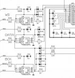
TDA1541A-MK7 schematics
Here are the latest TDA1541A-MK7 DAC concept schematics.
Active divider decoupling caps (C3 ... C16) have been changed to 1uF 1210 SMD film caps (Cornell Dubilier) that were specifically designed for decoupling and filter applications.
U7 and U8 form the new synchronous divide_by_4 circuit. R18 minimizes clock load of code flip-flop U8. R17 and R19 minimize ground-bounce. Output signals are tapped form U7, it drives DAC BCK input, DEM clock synchronizer, and DATA / WS synchronous reclockers.
The unusual powering of synchronous reclockers and divider are a result of long term listening tests and power supply noise / interference measurements. This concept offered best performance so far. All attempts based on (shunt) regulators failed, probably due to resulting noise / interference spectrum.
The MK6 module can be modified by adding an extra PCB, well if it can be called a PCB as it only measures 4 x 4mm. It contains extra D flip-flop U8.
Attachments
- Home
- Source & Line
- Digital Line Level
- Building the ultimate NOS DAC using TDA1541A