Re: 4 JFET amp schematic

Nelson Pass:
"Using a constant current source to bias the differential pair (I1) is probably the most key improvement. It has the advantage that it does not raise the open loop gain, but dramatically improves the power supply rejection (PSRR), making the performance independent of supply fluctuation and noise. It also greatly improves the common mode rejection (CMRR) of the input stage, typically by a factor of 20 to 30 dB."
-ecdesigns- said:Hi Radian,
......I removed the current source as performance significantly dropped (loss of dynamic resolution) when using one.
Nelson Pass:
"Using a constant current source to bias the differential pair (I1) is probably the most key improvement. It has the advantage that it does not raise the open loop gain, but dramatically improves the power supply rejection (PSRR), making the performance independent of supply fluctuation and noise. It also greatly improves the common mode rejection (CMRR) of the input stage, typically by a factor of 20 to 30 dB."
Hi Radian,
I was expecting this remark,
Needless to say I already thoroughly tested CCS instead of the resistors in this specific amplifier. Note that my main objective is to achieve highly transparent realistic sound quality. The amplifier should be able to process complex audio signals flawlessly, that's why I left-out global feedback as well.
Think of capacitance modulation (similar as with muting transistors on analogue outputs of CD players).
Nelson Pass:
"Using a constant current source to bias the differential pair (I1) is probably the most key improvement. It has the advantage that it does not raise the open loop gain, but dramatically improves the power supply rejection (PSRR), making the performance independent of supply fluctuation and noise. It also greatly improves the common mode rejection (CMRR) of the input stage, typically by a factor of 20 to 30 dB."
I was expecting this remark,
Needless to say I already thoroughly tested CCS instead of the resistors in this specific amplifier. Note that my main objective is to achieve highly transparent realistic sound quality. The amplifier should be able to process complex audio signals flawlessly, that's why I left-out global feedback as well.
Think of capacitance modulation (similar as with muting transistors on analogue outputs of CD players).
Cheers Ecdesigns
Thank-you for the detailed reply.
I have all of the parts for the sync reclocker, so it will be easy to try it out. I just need to get the flip flop and a couple of the 174 chips..............and then I would like to try one of your designs, as I have the 4 TDA1541s I guess that the DI4T would be the obvious choice.
From what you said in the reply I understand that the build is really 4 independent TDA1541 DACs with seperate PS and decoupling PLUS the seperate DEM clock module.
Cannot wait for the D14T boards.
Brad
Hi EC
Yoy said that 74xx74 is not the solution for the reclock...
Which f-f You suggest for that?
(If You dont mind...)
Yoy said that 74xx74 is not the solution for the reclock...
Which f-f You suggest for that?
(If You dont mind...)
Hi Zoran,
It works, but it's not the best chip for achieving lowest possible jitter amplitude.
It's also VERY important to use one single chip for reclocking the critical timing signal. NEVER reclock BCK, WS and DATA in the same chip as this causes unwanted crosstalk and increased jitter amplitude on the timing signal.
Same applies for I2S wiring / distribution, the DATA signal is a big interference source and measures should be taken in order to avoid crosstalk.
If you MUST use (synchronous) reclocking, I would suggest to use the Fairchild SN74F164. This is a shift-register, but contains usable cascaded D flip-flops. This chip provided lowest jitter amplitude during measurements.
Yoy said that 74xx74 is not the solution for the reclock...
Which f-f You suggest for that?
It works, but it's not the best chip for achieving lowest possible jitter amplitude.
It's also VERY important to use one single chip for reclocking the critical timing signal. NEVER reclock BCK, WS and DATA in the same chip as this causes unwanted crosstalk and increased jitter amplitude on the timing signal.
Same applies for I2S wiring / distribution, the DATA signal is a big interference source and measures should be taken in order to avoid crosstalk.
If you MUST use (synchronous) reclocking, I would suggest to use the Fairchild SN74F164. This is a shift-register, but contains usable cascaded D flip-flops. This chip provided lowest jitter amplitude during measurements.
Thanks EC,
I am using reclk, for years
and achieving noticeble better sonic results then one without...
(nos and 2x-4x os mode probes...)
maybe the speed is not a issue there
but it might be useful to try the NC7SZ74
i didnt yet...
I am using reclk, for years
and achieving noticeble better sonic results then one without...
(nos and 2x-4x os mode probes...)
maybe the speed is not a issue there
but it might be useful to try the NC7SZ74
i didnt yet...
Of course,
I didnt used the same chip for different d-lines...
The double f-f in one chip used, avoiding metastabile state,
2 serial f-f,
and -Q tap was very useful for overriding additional inverter in some
nos cases with BB format...
I didnt used the same chip for different d-lines...
The double f-f in one chip used, avoiding metastabile state,
2 serial f-f,
and -Q tap was very useful for overriding additional inverter in some
nos cases with BB format...
Hi Zoran,
Yes, when timing signals have high jitter amplitude (they usually have), synchronously reclocking these with a low jitter clock will usually provide better sonic results.
I haven't tested the Fairchild tiny-logic NC7SZ74K8X yet, but I have good results with the NC7SZ125P5X buffers.
Every gate adds jitter, but since clock buffering is required, at least one has to be added in series with the clock signal. But when using D flip-flops for synchronous reclocking, there are at least 2 inverting gates in the signal path (study D flip-flop logic diagram), these will also increase jitter amplitude when compared to a single gate clock buffer.
Typical D flip-flops will have 6 or more gates, these all switch and generate switching noise (ground bounce). I rather have one gate switching in a critical clock circuit than 12 (dual D flip-flop required for reducing effects of metastability).
When connecting both an inverting and a non inverting clock buffer to a masterclock, you will achieve the same with lower added timing jitter amplitude.
Distribution of clock signals often adds much more jitter than expected, poor clock routing can easily boost jitter amplitude to unexpected high levels.
I am using reclk, for years
and achieving noticeble better sonic results then one without...
Yes, when timing signals have high jitter amplitude (they usually have), synchronously reclocking these with a low jitter clock will usually provide better sonic results.
I haven't tested the Fairchild tiny-logic NC7SZ74K8X yet, but I have good results with the NC7SZ125P5X buffers.
Every gate adds jitter, but since clock buffering is required, at least one has to be added in series with the clock signal. But when using D flip-flops for synchronous reclocking, there are at least 2 inverting gates in the signal path (study D flip-flop logic diagram), these will also increase jitter amplitude when compared to a single gate clock buffer.
Typical D flip-flops will have 6 or more gates, these all switch and generate switching noise (ground bounce). I rather have one gate switching in a critical clock circuit than 12 (dual D flip-flop required for reducing effects of metastability).
and -Q tap was very useful for overriding additional inverter in some
nos cases with BB format...
When connecting both an inverting and a non inverting clock buffer to a masterclock, you will achieve the same with lower added timing jitter amplitude.
Distribution of clock signals often adds much more jitter than expected, poor clock routing can easily boost jitter amplitude to unexpected high levels.
Yes EC
I am keeping the mck, and all lines short as possibile
even without sheilded cable working stable...
thaks...
I am keeping the mck, and all lines short as possibile
even without sheilded cable working stable...
thaks...
DEM clock issues
Hi Telstar,
The DI4T main-board is causing problems, this has delayed DI4T PCB design. The problem is the DEM clock circuit. I am currently testing a differential DEM clock injector that drives both pin 16 and pin 17 of each TDA1541A chip.
Hi Telstar,
The DI4T main-board is causing problems, this has delayed DI4T PCB design. The problem is the DEM clock circuit. I am currently testing a differential DEM clock injector that drives both pin 16 and pin 17 of each TDA1541A chip.
Re: DEM clock issues
Thank you for the reply!
I'm not in a hurry anyway.
-ecdesigns- said:Hi Telstar,
The DI4T main-board is causing problems, this has delayed DI4T PCB design. The problem is the DEM clock circuit. I am currently testing a differential DEM clock injector that drives both pin 16 and pin 17 of each TDA1541A chip.
Thank you for the reply!
I'm not in a hurry anyway.
No opamps!
Sound: I don't have words.
Looks: ugly--> http://picasaweb.google.com/lh/photo/Yih4A3m84IrZwvcNQCmC9g
No opamps, no feedback, no filter...
Now, the "scrambler".
Bye,
M
Sound: I don't have words.
Looks: ugly--> http://picasaweb.google.com/lh/photo/Yih4A3m84IrZwvcNQCmC9g
No opamps, no feedback, no filter...
Now, the "scrambler".
Bye,
M
Hi John
Thank you for info
Still waiting for your DI4T
Hi Max
thats mean best or worst 😀
Best regards, jeffry
Thank you for info
Still waiting for your DI4T
Hi Max
thats mean best or worst 😀
Best regards, jeffry
Hi Jeffry,
 Please, I'm trying to refrain myself from going into audiophile hyperboles...I realized that, being myself a self-restrained man, the more exited I get about a subject the more I lose in credibility...
Obviously better 😉
Try the Ultimate NOS DAC, which is the real name of this invention.
Cheers,
M
Please, I'm trying to refrain myself from going into audiophile hyperboles...I realized that, being myself a self-restrained man, the more exited I get about a subject the more I lose in credibility... Obviously better 😉
Try the Ultimate NOS DAC, which is the real name of this invention.
Cheers,
M
Hello ECdesigns (John)
Have you changed something on the dem reclock schematics? I tried a dem reclock on a CD880 but hear digital noise on the background. (Kwak, /4 HCT161 divider and then a /16 give 176kHz. 150p coupling cap to pin 16. Do you have any tips?
Thanks for your precious time.
Are you designing a compact TDA1543 nonos dac pcb?
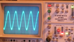
DI4T 1KHz -60dB sinewave oscillogram
Hi tubee,
I use 352.8 KHz DEM clock, and use 1nF coupling caps feeding a differential DEM clock signal into both pin 16 and pin 17.
The DEM clock source needs to generate both an inverted and non-inverted low jitter clock signal of 352.8 KHz. So you could use a divide-by-8 counter and a suitable inverter to create both required clock signals.
I connected both outputs to 1K2 series resistors that feed a 330 Ohm load resistor. The attenuated ac voltage across the 330 Ohm resistor is then coupled into pins 16 and 17 using 1nF ceramic NPO SMD caps.
When the TDA1541A is implemented correctly, and the DEM clock works as planned, there should be no audible noise at all.
The active divider decoupling pins (the ones connected to the 14 decoupling caps) are very sensitive, and can easily pick-up hum and noise, even with the decoupling caps connected.
The higher the decoupling cap value (1 ... 2.2uF for example), the less problems with this. The connections of the decoupling caps should be kept as short as possible, preferably a few millimeters maximum. It also helps to use a screen around the decoupling caps and traces.
Correct DEM functioning can be verified by playing back a 1 KHz 0dB sinewave signal. I attached an oscillogram of DI4T 1 KHz -60dB sinewave output signal I just made this morning.
Yes, it's the DI4MJ (posted a picure of the early prototype PCB some time ago). After a lot of different DI DAC designs and many experiments, I plan to stick with 2 "final" DI DAC designs, the DI4MJ (4 x TDA1543), and the DI4T (4 x TDA1541A).
The DI DACs use 4 x interpolation, and produce an output signal with 176.4 KHz sample rate, so strictly speaking both DI4T and DI4MJ are OS DACs that share similarities with NOS DACs (no brickwall filtering).
Hi tubee,
Have you changed something on the dem reclock schematics? I tried a dem reclock on a CD880 but hear digital noise on the background. (Kwak, /4 HCT161 divider and then a /16 give 176kHz. 150p coupling cap to pin 16. Do you have any tips?
Thanks for your precious time.
I use 352.8 KHz DEM clock, and use 1nF coupling caps feeding a differential DEM clock signal into both pin 16 and pin 17.
The DEM clock source needs to generate both an inverted and non-inverted low jitter clock signal of 352.8 KHz. So you could use a divide-by-8 counter and a suitable inverter to create both required clock signals.
I connected both outputs to 1K2 series resistors that feed a 330 Ohm load resistor. The attenuated ac voltage across the 330 Ohm resistor is then coupled into pins 16 and 17 using 1nF ceramic NPO SMD caps.
When the TDA1541A is implemented correctly, and the DEM clock works as planned, there should be no audible noise at all.
The active divider decoupling pins (the ones connected to the 14 decoupling caps) are very sensitive, and can easily pick-up hum and noise, even with the decoupling caps connected.
The higher the decoupling cap value (1 ... 2.2uF for example), the less problems with this. The connections of the decoupling caps should be kept as short as possible, preferably a few millimeters maximum. It also helps to use a screen around the decoupling caps and traces.
Correct DEM functioning can be verified by playing back a 1 KHz 0dB sinewave signal. I attached an oscillogram of DI4T 1 KHz -60dB sinewave output signal I just made this morning.
Are you designing a compact TDA1543 nonos dac pcb?
Yes, it's the DI4MJ (posted a picure of the early prototype PCB some time ago). After a lot of different DI DAC designs and many experiments, I plan to stick with 2 "final" DI DAC designs, the DI4MJ (4 x TDA1543), and the DI4T (4 x TDA1541A).
The DI DACs use 4 x interpolation, and produce an output signal with 176.4 KHz sample rate, so strictly speaking both DI4T and DI4MJ are OS DACs that share similarities with NOS DACs (no brickwall filtering).
Attachments
Ok thanks John for reply and help. Just checked everything: all seems fine, it must be the dem. The noise sounds like a bad adjusted pcm56, MSB noise, so could be the dividercaps also. Refitted MSB and the one near that with epcos 1Uf and 0.47uF. Refitted a 470p dem cap: enormous noise appeared. Will try a dem schematic you suggesting, and check divider caps. Sorry for ot.
A drawing says more then 1000 words
Like this John? http://img147.imageshack.us/img147/1883/demreclockfg7.jpg
Like this John? http://img147.imageshack.us/img147/1883/demreclockfg7.jpg
Hi tubee,
DEM clock issues usually don't cause enormous noise levels. Seems like one of the active divider decoupling pins makes short circuit with other traces, this would produce clearly audible noise.
TDA1541A (analogue) ground routing has big impact on performance, try to use pin 5 as star ground, and route all AGND connections straight to this pin. The active divider outputs are VERY sensitive to external (electromagnetic) noise sources or leakage currents (50 mega-ohms to GND is sufficient to introduce severe bit errors!). Try to keep decoupling cap traces very short, and use sufficient screening (filled ground plane underneath the decoupling caps). It could even be necessary to put copper foil screens around the decoupling caps, and connect these to AGND too.
Yes, that's correct.
Refitted a 470p dem cap: enormous noise appeared
DEM clock issues usually don't cause enormous noise levels. Seems like one of the active divider decoupling pins makes short circuit with other traces, this would produce clearly audible noise.
TDA1541A (analogue) ground routing has big impact on performance, try to use pin 5 as star ground, and route all AGND connections straight to this pin. The active divider outputs are VERY sensitive to external (electromagnetic) noise sources or leakage currents (50 mega-ohms to GND is sufficient to introduce severe bit errors!). Try to keep decoupling cap traces very short, and use sufficient screening (filled ground plane underneath the decoupling caps). It could even be necessary to put copper foil screens around the decoupling caps, and connect these to AGND too.
http://rapidshare.de/files/40919911/HDEND_-_Audiophile_Air2.part2.rar.html
Yes, that's correct.
- Home
- Source & Line
- Digital Line Level
- Building the ultimate NOS DAC using TDA1541A