Dem Clock feeding
Hi John (ECdesigns)
Did you try as we discussed a couple of month ago to feed the dem input (pin 16 and 17) differential with a coil tuned on 352 Khz (mf trafo f.i. Toko) (in Dutch middenfrequent trafo) instead of an inverter ?
Onno
Hi John (ECdesigns)
Did you try as we discussed a couple of month ago to feed the dem input (pin 16 and 17) differential with a coil tuned on 352 Khz (mf trafo f.i. Toko) (in Dutch middenfrequent trafo) instead of an inverter ?
Onno
bit of topic
Hi Tubee
do you have the servicemanual for the CD880 ? (or cd882)
If so I like to get it
Thanks in advance for answering.
Onno
tubee said:Hello ECdesigns (John)
Have you changed something on the dem reclock schematics? I tried a dem reclock on a CD880 but hear digital noise on the background. (Kwak, /4 HCT161 divider and then a /16 give 176kHz. 150p coupling cap to pin 16. Do you have any tips?
Thanks for your precious time.
Are you designing a compact TDA1543 nonos dac pcb?
Hi Tubee
do you have the servicemanual for the CD880 ? (or cd882)
If so I like to get it
Thanks in advance for answering.
Onno
Hi Jean-Paul,
i contact to John and he said you was in his place and listening to newest audio set (of course new DI4T).
Could you share some sonic impressions?
I dont have that chance (1300km distance).
Best regards,
Bostjan
i contact to John and he said you was in his place and listening to newest audio set (of course new DI4T).
Could you share some sonic impressions?
I dont have that chance (1300km distance).
Best regards,
Bostjan
Dear -ecdesigns-
Given the discrete 4FEt differential amp circuit as is on post #2239, what would be the minimum IDSS that you would recommend for each FET of the differential pair?
I happen to have many matched 2SK170, GR type, from 2.2 to 4mA...
Thanks,
M
PS: yes, I am about to build my next couple of DI4M 😉
Oh, and one with "the scrambler" 😎
Onnosr said:bit of topic
Hi Tubee
do you have the servicemanual for the CD880 ? (or cd882)
If so I like to get it
Thanks in advance for answering.
Onno
Tubee !
Many thanks !!
Onno


I am thinking about linearizing the individual bits of the DAC by deliberately introducing leakage currents at the active divider filter pins. The ultimate goal would be to achieve S1 or even S2 performance. The only parameter mentioned in the data sheet that makes the difference is linearity error.-ecdesigns- said:The active divider outputs are VERY sensitive to external (electromagnetic) noise sources or leakage currents (50 mega-ohms to GND is sufficient to introduce severe bit errors!).
oshifis said:I am thinking about linearizing the individual bits of the DAC by deliberately introducing leakage currents at the active divider filter pins. The ultimate goal would be to achieve S1 or even S2 performance. The only parameter mentioned in the data sheet that makes the difference is linearity error.
I tried to inject current into the MSB pin.
Something like 10meg 1meg-pot 10meg to manipulate the voltage that can be measured on the pin.
Caused only distortion.
Maybe of was not fine enough.
Did not have much motivation.
Hi tubee,
TDA1541A chips are quite rigid and can withstand "accidents" without damage.
If you capacitively couple the DEM clock signal to the DAC chips, using 1nF capacitors, there is very little that could go wrong.
IF a TDA1541A is permanently damaged, it's usually caused by power supply issues, exceeding absolute maximum ratings, or overheating during long time periods.
The new DEM clock circuit I described was thoroughly tested and has proven to work fine. The resistive attenuator makes sure that both voltage and current are limited, so the on-chip DEM clock oscillator circuit won't be overloaded.
Guys: BEWARE with DEM stuff reclocking and so on. I just SMOKED a single crown....
TDA1541A chips are quite rigid and can withstand "accidents" without damage.
If you capacitively couple the DEM clock signal to the DAC chips, using 1nF capacitors, there is very little that could go wrong.
IF a TDA1541A is permanently damaged, it's usually caused by power supply issues, exceeding absolute maximum ratings, or overheating during long time periods.
The new DEM clock circuit I described was thoroughly tested and has proven to work fine. The resistive attenuator makes sure that both voltage and current are limited, so the on-chip DEM clock oscillator circuit won't be overloaded.
Hi oshifis,
The outputs of the active dividers don't require any adjustment when the DEM clock is working correctly. It's possible to make "corrections" on the 6 MSBs of each channel, using and external variable precision constant current source that thermally tracks the TDA1541A internal current reference source. Corrective currents should be in the range of approx. 61 nA, needless to say that this is going to be very difficult, and is likely to introduce more errors.
It's better to try improve DEM clock performance, and optimize both decoupling caps and ground traces. Like coupling caps, every DEM clock capacitor type and value will have different effect on sound quality. It seems that decoupling capacitor value needs to be accurately tuned to the DEM clock frequency. Too high decoupling cap values on the MSBs will usually result in a slow laid-back sound. Too low decoupling cap values will usually result in over bright, slightly distorted sound. The trick is to find the optimal value for the decoupling caps.
Also keep in mind that bit 12, 14, and 16 ripple current frequency equals fDEM/2, this is due to paralleling of active divider outputs for these bits (explained in TDA1541(A) functional description). This means that decoupling caps on these pins need to have twice the capacitance compared to the remaining caps.
If the specified 100nF decoupling cap value at approx. 200 KHz DEM clock is correct, the following standard decoupling capacitance values would be required for a 352.8 KHz DEM clock:
bits 12, 14, 16 > 120nF
bits 10, 11, 13, 15 > 68nF
I am thinking about linearizing the individual bits of the DAC by deliberately introducing leakage currents at the active divider filter pins. The ultimate goal would be to achieve S1 or even S2 performance. The only parameter mentioned in the data sheet that makes the difference is linearity error.
The outputs of the active dividers don't require any adjustment when the DEM clock is working correctly. It's possible to make "corrections" on the 6 MSBs of each channel, using and external variable precision constant current source that thermally tracks the TDA1541A internal current reference source. Corrective currents should be in the range of approx. 61 nA, needless to say that this is going to be very difficult, and is likely to introduce more errors.
It's better to try improve DEM clock performance, and optimize both decoupling caps and ground traces. Like coupling caps, every DEM clock capacitor type and value will have different effect on sound quality. It seems that decoupling capacitor value needs to be accurately tuned to the DEM clock frequency. Too high decoupling cap values on the MSBs will usually result in a slow laid-back sound. Too low decoupling cap values will usually result in over bright, slightly distorted sound. The trick is to find the optimal value for the decoupling caps.
Also keep in mind that bit 12, 14, and 16 ripple current frequency equals fDEM/2, this is due to paralleling of active divider outputs for these bits (explained in TDA1541(A) functional description). This means that decoupling caps on these pins need to have twice the capacitance compared to the remaining caps.
If the specified 100nF decoupling cap value at approx. 200 KHz DEM clock is correct, the following standard decoupling capacitance values would be required for a 352.8 KHz DEM clock:
bits 12, 14, 16 > 120nF
bits 10, 11, 13, 15 > 68nF
Hi -ecdesigns-
How did it go? 🙂
Just in case you did not see my last question...
Thanks again,
M
How did it go? 🙂
Just in case you did not see my last question...
Dear -ecdesigns-
Given the discrete 4FEt differential amp circuit as is on post #2239, what would be the minimum IDSS that you would recommend for each FET of the differential pair? I happen to have many matched 2SK170, GR type, from 2.2 to 4mA... Thanks, M
Thanks again,
M
Hi maxlorenz,
If you are referring to the demonstration of my audio set on the 19th, I suggest to wait for the review to be published.
This depends on the JFET characteristics, I run the differential input pair in the DI4MJ at approx. 200uA for each FET. I used dual SMD JFETs from NXP (PMBFJ620). These are low noise, high gain RF JFETs.
How did it go? 🙂
If you are referring to the demonstration of my audio set on the 19th, I suggest to wait for the review to be published.
Given the discrete 4FEt differential amp circuit as is on post #2239, what would be the minimum IDSS that you would recommend for each FET of the differential pair?
This depends on the JFET characteristics, I run the differential input pair in the DI4MJ at approx. 200uA for each FET. I used dual SMD JFETs from NXP (PMBFJ620). These are low noise, high gain RF JFETs.
Guys: I am happy.
The S1 dac is still working, there was a small fuse broken (oxidised, not melted) to the I/V section.)
Must have some serious because i did'nt discover that before 😉
The S1 dac is still working, there was a small fuse broken (oxidised, not melted) to the I/V section.)
Must have some serious
because i did'nt discover that before 😉Hi all,
Project update,
I finally decided to go for a modular DI4T main board. All major circuits are now placed on small modules. This provides easy upgrading, troubleshooting and repair, and enables higher performance.
I split-up the main electronics in 4 modules, I attached a picture of these modules. Each module measures 0.82" (2.1cm) x 2" (5.1cm), and has an 8-way pin header on each side. The modules can also be used for other projects.
The one on the left is a complete SPDIF receiver module, based on a CS8416. The Toslink optical receiver module RX177L can be directly connected as the SPDIF receiver module has both an integrated SPDIF attenuator, and a capacitive coupling to RXP and RXN inputs. The loop filter is optimized for lowest jitter in order to prevent data corruption. Mode set resistors are included too, the module is set for slave-clock mode and I2S output. The integrated Micrel ultra low noise 3.3V LDO regulator (specified @ 260nV SQRT Hz) provides a clean power supply for the receiver chip.
Module connections: GND, VCC, SPDIF input, BCK input, WS input, DATA output and MCK output.
The next one is the Micro-controller-based tracker module. It's basically a Microchip controller, a discrete 10-bit R2R DAC, built using 0.1% SMD resistors, and a low capacitance output filter. The R2R DAC provides an analogue control voltage to tune the VCXO master clock module. The MCK input provides the source clock frequency reference, while the BCK input provides the master clock frequency reference. The micro-controller also runs on BCK (2.8224 MHz), so inter-modulation between multiple clocks is prevented. The module provides a "locked" output that indicates when the tracker has locked to the digital audio source.
Module connections: GND, VCC, MCK input, BCK input, Locked output and analogue control voltage output.
Next one is the master clock module, this module holds a discrete VCXO oscillator, and 4 ultra high speed separate clock buffers. The master clock generates 2.8224 MHz and has a pulling range of approx. 100ppm. The super cap is also integrated on this module. The low capacitance control voltage filter blocks unwanted interference. I wasn't able to measure any jitter with my measuring instruments when running this VCXO module on the novel charge-transfer power supply.
Module connections: GND, VCC, analogue control voltage input, and 4 buffered clock outputs.
The module on the right holds a 4 x interpolator, scrambler, WS, and differential DEM clock generator. The circuit is built around 4 x 64-bit shift-registers, counters, multiplexer, and inverters. The outputs have resistors installed that are part of the I2S input attenuators.
Module connections: GND, VCC, DATA input, BCK input, WS output, DEM output, NDEM output, WS16 output, WS32 output, WS48 output, WS64 output, DATA16 output, DATA32 output, NDATA48 output and NDATA64 output.
I already blocked source jitter, but I didn't block mains noise. Clean power supplies turned out to be just as important as low timing jitter. Battery power supplies have the potential of providing a clean power supply voltage, but using batteries can be rather problematic.
First I had the illusion that a super regulator could solve this mains noise issue, it turned out it can't. The noise still enters through the multiple closed current paths between transformer, connected electronics, and connected equipment (amplifiers, CD players, Computers). The noise causes both DC and ac voltage drops across GND, that are then added to the clean super reg output, resulting in virtually similar noise levels at the load. Even worse is that the current path often extends to connected equipment, causing even more problems.
So I figured the only way to get rid of the mains noise was to completely interrupt the current paths between transformer and electronics while still transferring the required energy. In other words, I had to transfer energy from transformer to load without actually connecting both.
Well I have come up with a suitable solution, the charge-transfer power supply. It completely interrupts the current path between both transformer and load (blocking mains noise) while still transferring energy from the mains power supply to the load.
Attachments

This guy is amazing...I only could finish soldering the prototype scrambler-interpolator and he came out with a complete new modular configuration plus a brilliant idea for a clean power supply! 
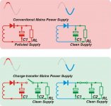
Charge-transfer power supply basics
Hi maxlorenz,
At first I tried all the tricks that are commonly used in an attempt to obtain clean power supplies (Schottky diodes, exotic caps, filters, ultra-low noise voltage regulators, super regulators, gyrators and so on). But compared to a good battery power supply, all these tricks simply seemed to fail.
I spend quite some time figuring out what caused this, why does a battery power supply work so much better, despite comparable noise levels?
It appears to be the pollution on the supply current path, a battery creates a pure DC supply current path, while a mains voltage creates both a DC and ac (pollution) current path at the same time. Since this current runs through all connected electronic circuits, it pollutes all.
So I attempted to mimic a battery power supply using a mains power supply. My batteries are electrolytic caps, and they are depleted within a few hundred milliseconds, so they need to be charged frequently, 50 ... 120 times a second. This is done by using an electronic power switch that is operated at the mains frequency (half-wave rectifier), or double mains frequency (full-wave rectifier). The trick is to charge this capacitor without introducing the unwanted polluted current path between transformer and load.
They say that a picture tells more than a thousand words, so I added a simple basic schematic of both a conventional mains power supply, and the new charge-transfer power supply.
I used the red color to indicate the polluted current path, and the green color to indicate the clean current path. The dark red color at the peak of the sine-wave illustrates the charge current flow, the electronic switch is OPEN during this short charge cycle.
The blue color indicates no current flow (rectifier diodes are not conducting). This basically means that the unwanted charge current path is interrupted (open circuit) during this time
These charge-transfer power supplies seem to be able to mimic a very good battery power supply, while running on a heavily polluted mains power supply.
I already tested 3 of these charge-transfer power supplies (+10V, -10V, and -20V) in the DI4T, the impact on sound quality could best be described using your phrase "I have no words ....".
Hi maxlorenz,
plus a brilliant idea for a clean power supply!
At first I tried all the tricks that are commonly used in an attempt to obtain clean power supplies (Schottky diodes, exotic caps, filters, ultra-low noise voltage regulators, super regulators, gyrators and so on). But compared to a good battery power supply, all these tricks simply seemed to fail.
I spend quite some time figuring out what caused this, why does a battery power supply work so much better, despite comparable noise levels?
It appears to be the pollution on the supply current path, a battery creates a pure DC supply current path, while a mains voltage creates both a DC and ac (pollution) current path at the same time. Since this current runs through all connected electronic circuits, it pollutes all.
So I attempted to mimic a battery power supply using a mains power supply. My batteries are electrolytic caps, and they are depleted within a few hundred milliseconds, so they need to be charged frequently, 50 ... 120 times a second. This is done by using an electronic power switch that is operated at the mains frequency (half-wave rectifier), or double mains frequency (full-wave rectifier). The trick is to charge this capacitor without introducing the unwanted polluted current path between transformer and load.
They say that a picture tells more than a thousand words, so I added a simple basic schematic of both a conventional mains power supply, and the new charge-transfer power supply.
I used the red color to indicate the polluted current path, and the green color to indicate the clean current path. The dark red color at the peak of the sine-wave illustrates the charge current flow, the electronic switch is OPEN during this short charge cycle.
The blue color indicates no current flow (rectifier diodes are not conducting). This basically means that the unwanted charge current path is interrupted (open circuit) during this time
These charge-transfer power supplies seem to be able to mimic a very good battery power supply, while running on a heavily polluted mains power supply.
I already tested 3 of these charge-transfer power supplies (+10V, -10V, and -20V) in the DI4T, the impact on sound quality could best be described using your phrase "I have no words ....".
Attachments
Hi John.
Is the PS thing your invention? You should be careful then, other people might steal your ideas. 😉
I am still loving my batteries with TeddyRegs. I think low impedance is the key.
However, sooner or later I need try your approach.
Anyhow:
I would love to get the receiver and clock modules to try them on my different
DACS and to compare them with USB. ( I can come by and pick them up 😀 - beside that
I can listen to the DI4 - you might want to PM me.)
Cheers
Klaus
- Home
- Source & Line
- Digital Line Level
- Building the ultimate NOS DAC using TDA1541A