I mean when making a pcb, one needs to think of things connected to a "NET".
You, you want planes for the net's with the following Pin Labels on the IC
Digital plane pair (top of PCB under TDA1541 only:
DGND (net Pin 14)
+5V (net Pin 28)
The net Pin 15 plane is also extended to the source circuitry or off board connectors.
Analogue plane pair:
AGND (net Pin 5)
-15V (Net Pin 15)
The main reference plane for all analogue pin's is Net pin 15.
As several pin's combine multiple function onto one pin this gets interesting.
In this case priority is given to analogue loops.
Digital inputs get priority on the top with Net pin 14 plane
Thor
This is terrible mantra, no ground, I can go outside the sofa ! 😱
thanks for the longer answer.
We should for everyone talk with the pins number of the datasheet and NET pcb connection concept ! Okay, I am reassured it flow back to a "cold" layer.
I like a lot the reverse polarity illustration, very didactic , thanks ! 🙂
thanks for the longer answer.
We should for everyone talk with the pins number of the datasheet and NET pcb connection concept ! Okay, I am reassured it flow back to a "cold" layer.
I like a lot the reverse polarity illustration, very didactic , thanks ! 🙂
So, that's the current drawing board:
PS, of course I considered a folded cascode from the negative rail, but where is the benefit?
Maybe if we split the current so half the current goes to the designated output pin which is "agnd" referenced and half is mirrored again on the positive rail and goes to the same output, we have 2V directly to ground.
Lots of extra effort, and where is the befit?
Thor

This is terrible mantra, no ground, I can go outside the sofa ! 😱
It is strictly speaking also true in that sense.
Worse news. There also is no sofa. There is nothing
Only 99.9% empty space and forces... Solid objects are another left wingnut conspiracy, they are illusions.
Open your mind!
question of scale only ! Uh time I mean....hummmm, uh, a little of both, but please brake if you see a wall. Not always easy to flow between particles !
These tests are simulations. And with questionable spice model 431 in that time. I knew it probably for 20 years. When the first versions of pspice emerged... 🙁Detailed tests and sim's on TL431, quite vintage.
TNT-Audio Simple Voltage Regulators Part 2.2: Output Impedance (TL 431)
I just check the set ups and the results are not matching... Even a some sim tests are done wrong.
.
For instance when putting the abstract current source as current limiter versus simple resistor doing the same - results are dramatically different. (Results will be different with active current limiter too...)
.
And in some tests for 100mA current small BJT shunt transistor running at more than 1W power from 500mW as max.
red is abstract current source
But I reduced and the version for fixed values. I put BC560C as standard transistor but others can be used. It is not critical. Others shoud be as writen for same chrs. And this is the minimal configutarion for the solid results.
.
The small decoupling C after 431 is behaving different with some models. TL431ED from Eugene is for now most accurate model... But again Zetex is official model? So I put booth values of this C.


.
The small decoupling C after 431 is behaving different with some models. TL431ED from Eugene is for now most accurate model... But again Zetex is official model? So I put booth values of this C.
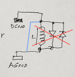
@ThorstenL
Thor, I have one question please.
The idea is about -5V supply:
Because it is in the same time analog and digital
To made 2 independent power supplies for.
one coming from analog transformer thae samw one to feed -18V analog
other from digital +5V
.
Like this
?
Thanks
.

Thor, I have one question please.
The idea is about -5V supply:
Because it is in the same time analog and digital
To made 2 independent power supplies for.
one coming from analog transformer thae samw one to feed -18V analog
other from digital +5V
.
Like this
?
Thanks
.
Bead+diodes = was popular in 80/90th, you can find it even in app.notes from AD, TI, etc.
But this is wrong.
Another erroneous trend in the past was to connect AGND and DGND at the power supply inputs to the ADC/DAC board.
Nowadays, AGND and DGND are connected under or near the ADC/DAC chip.
So:
But this is wrong.
Another erroneous trend in the past was to connect AGND and DGND at the power supply inputs to the ADC/DAC board.
Nowadays, AGND and DGND are connected under or near the ADC/DAC chip.
So:
Attachments
That is a bad way of thinking, at least in the sense where it is of utmost importance where/how current flows/makes a loop. If you let current from digital flow trough analog to make a loop, you messed it up, lots of noise introduced. You can't just slap it under or wherever and call it a day, or nowadays at that.
It is necessary to understand where which currents flow, and to avoid crossing and joint flow of digital/analog and signal/supply currents.
Alex.
Alex.
These tests are simulations. And with questionable spice model 431 in that time. I knew it probably for 20 years. When the first versions of pspice emerged... 🙁
I know. However, we can also do a simple calculation as a Sziklai Pair.
The transconductance of the TL431 is ~6,666mA/V.
The transconductance of a BD139 with a 220R base resistor running at 50mA is ~ 360mA/V.
Combined as Sziklai we have in theory 2.4kA/V transconductance. That's ~5mOhm ESR.
In reality my "milkmaid" calculation is optimistic. I use the TI model in TINA-TI, which is not accurate, but accurate enough for SMPS control loops.
So we should get a ESR of ~5...35mOhm for MY design with BD140 (with TO220 Heatsink) or BCP53 for a SMT PCB with suitable copper area.
So I got Edmonds model into TINA-TI (use the .sub file renamed to .cir) here my result with a simple RLC model of the output Os-Con and a LM317 Model from TI (transient PSPICE).
All Graphs are from +5V to -15V (the whole stack).
Output impedance:
Seeing ~9mOhm, for 3 regulators in series, seems my "milkmaid" calculations are within 3dB. There are advantages growing up with a slipstick.
PSRR for 100mV source on 42V DC:
At 77kHz we still get almost 90dB noise reduction, for 100Hz it's almost 160dB. More than good enough.
Noise:
Around 54uV in a 100kHz bandwidth across the whole stack, 43uV across the 15V branch, so noise contribution to the output at the TDA1541 ~151dB below 0dBFS, or as I prefer to say "a tiny fraction of feck all".
So, 9mOhm ESR at low enough frequencies, noise in system 150dB below full scale and nearly 160dB attenuation of mains ripple and nearly 90dB attenuation of common off-mains SMPS (on top of all passive filtering) I think even this power supply is way overbuild and way over specified for the job.
Do we really make it more complicated than this?
Thor
Bead+diodes = was popular in 80/90th, you can find it even in app.notes from AD, TI, etc.
But this is wrong.
Depends.
It is only wrong if the IC is designed with multiple Vss pin's that all act as Vss. Then yes, these should be connected together through an image plane and tightly coupled (use thin pre-preg between the planes not core) to the Vcc image plane.
Another erroneous trend in the past was to connect AGND and DGND at the power supply inputs to the ADC/DAC board.
Nowadays, AGND and DGND are connected under or near the ADC/DAC chip.
So:
No, I disagree FOR TDA1541 ONLY!!!
I explicitly set out my reasoning based on the TDA1541 internal design previous in the thread.
The pin called DGND on the TDA1541 is actually the -5V supply Pin for the internal CML/ECL logic and +5V is both the Audio Ground (or at least the return for the inverted signal current of both DAC channels - 8mA PP at 0dBFS) and the logic "ground" for the CML/ECL internal logic.
BUT DGND is also the reference point for the TTL2ECL input circuitry of the digital section.
The pin called AGND is actually a reference pin and the POSITIVE SUPPLY of the current sinks (including the DEM circuitry) while the -15V Pin is the ACTUAL common/return of the current sinks and thus the true AGND.
If you link pin's labelled AGND and DGND for the TDA1541 (and ONLY this IC) you are forcing an overall subideal design of the actual current loops in circuit.
So treat DGND on TDA1541 as -5V supply and +5V on TDA1541 as one of two analogue returns with a 20V DC difference but requiring essentially 0V AC difference.
Thor
@ThorstenL
Thor, I have one question please.
The idea is about -5V supply:
Because it is in the same time analog and digital
Actually, BEST I CAN TELL it is NEITHER part of the analogue current sinks nor of the digital logic.
I cannot say for sure, but I suspect it is "ballast" for the bit switches. Non of the literature gives any hint on what this does, so I THINK at least from the rest of the design it power a bunch of current sinks that "ballast" differential logic with outputs that must go below AGND to turn one bit switch off reliably.
The high current also suggests this, as we would have 16 X 2 switches where we likely see significant current.
To made 2 independent power supplies for.
Only 1 Pin.
Analysing dozens of service manuals, I usually find -5V generated from the same winding as +5V and -15V via the analogue circuitry.
But I always see -5V decoupled to AGND not DGND including in designs that separate AGND & DGND.
This again makes sense if -5V biases the bitswitches. A separate supply makes no sense to me.
Thor
9mOhm? Is very close to that I measured for DC for my TL431 supplies (near 10mOhm), but I used 120R instead of 510R for the resistor for B-E of the output transistor.I know. However, we can also do a simple calculation as a Sziklai Pair.
The transconductance of the TL431 is ~6,666mA/V.
The transconductance of a BD139 with a 220R base resistor running at 50mA is ~ 360mA/V.
Combined as Sziklai we have in theory 2.4kA/V transconductance. That's ~5mOhm ESR.
In reality my "milkmaid" calculation is optimistic. I use the TI model in TINA-TI, which is not accurate, but accurate enough for SMPS control loops.
So we should get a ESR of ~5...35mOhm for MY design with BD140 (with TO220 Heatsink) or BCP53 for a SMT PCB with suitable copper area.
View attachment 1349932
So I got Edmonds model into TINA-TI (use the .sub file renamed to .cir) here my result with a simple RLC model of the output Os-Con and a LM317 Model from TI (transient PSPICE).
All Graphs are from +5V to -15V (the whole stack).
Output impedance:
View attachment 1349935
Seeing ~9mOhm, for 3 regulators in series, seems my "milkmaid" calculations are within 3dB. There are advantages growing up with a slipstick.
PSRR for 100mV source on 42V DC:
View attachment 1349936
At 77kHz we still get almost 90dB noise reduction, for 100Hz it's almost 160dB. More than good enough.
Noise:
View attachment 1349937
Around 54uV in a 100kHz bandwidth across the whole stack, 43uV across the 15V branch, so noise contribution to the output at the TDA1541 ~151dB below 0dBFS, or as I prefer to say "a tiny fraction of feck all".
So, 9mOhm ESR at low enough frequencies, noise in system 150dB below full scale and nearly 160dB attenuation of mains ripple and nearly 90dB attenuation of common off-mains SMPS (on top of all passive filtering) I think even this power supply is way overbuild and way over specified for the job.
Do we really make it more complicated than this?
Thor
it is usuall "praxis" but without reading the datasheets? In every datasheet is clearly noted what value is max. allowed for AGND and DGND...Nowadays, AGND and DGND are connected under or near the ADC/DAC chip.
So the grounds, IF the pot dif. is in range, can be unconnected.
.
(As it noted many times before, TDA1541A has different internal structre)
.
Additional care should be taken in case of using separate transformer for PS for A and D sections
Because if the cgases grounds and/or screens are diferently conected, at the grounds could be potential and huge one probably in HF region. And that can kill the chip... 🙁
.
Because of that and because of less expensive way to go for one PS for A and D it is presenting as "better" way.
Last edited:
Yes 1merged into 1 pin -5V, but diferent "0". You can decouple -5V for dedicated "0", which one find more apropriate, or booth?Only 1 Pin.
Analysing dozens of service manuals, I usually find -5V generated from the same winding as +5V and -15V via the analogue circuitry.
But I always see -5V decoupled to AGND not DGND including in designs that separate AGND & DGND.
This again makes sense if -5V biases the bitswitches. A separate supply makes no sense to me.
Thor
The decouplig schematic is remain the same.
It is only separate "0" the -5V is common?
.
And it is multifunctional - easy to adopt for other types of DACs...
It is worth trying to me?
.
I will try to make sch with Your decoupling SCH, maybe it would be more clear.
Thanks
.
Of course, it is necessary to read both datasheets and application notes, but remember that views are changing.it is usuall "praxis" but without reading the datasheets?
More progressive methods of measurements and simulations are also appearing.
The EMC environment "around" is also changing.
Alex.
Yes 1merged into 1 pin -5V, but diferent "0". You can decouple -5V for dedicated "0", which one find more apropriate, or booth?
In my interpretation DGND is strictly related to the CML/ECL logic between +5V and DGND.
As said multiple times, as all Power/Gnd Pin's are Multi-domain on the TDA1541 using super capacitor chains or shunt regulator chains strike me as the best solution to, if necessary link all currents and make them complete their loops locally around the TDA1541 without "escaping" anywhere else.
Again, I see no benefit to making things more complex. I have been simulating my supercapacitor supplies and they really limit whatever currents can create as noise. I may not even bother separating DGND (-5V Vecl) physically from AGND as it typically is pretty quiet and DGND should see no current induced by the digital signals after conditioning.
Equally, the "ballast current" section in my analogue stage works fine, but the difference in 100's uV of error voltage vs 100's of nV, either one being low enough to not matter in practice.
I think you suggest a separate +/-5V supply linked to DGND and a -5V/-15V supply linked to AGND that link together at the -5V pin (and AGND - DGND linkage?).
If we can prove that -5V has sections that loop significant current to DGND and others to AGND, then by all means separate them out. I just don't see it, I really think the -5V Pin is just a Current Source/Sink power in.
And it is multifunctional - easy to adopt for other types of DACs...
I suggest against doing universal things. Optimise for one job and one job only.
Thor
- Home
- Source & Line
- Digital Line Level
- Building the ultimate NOS DAC using TDA1541A