Of course, it is necessary to read both datasheets and application notes, but remember that views are changing.
The TDA1541 is non-applicable to views created by CMOS logic. The number of FET's in the TDA1541 is zero and the number of PNP Transistors is miniscule.
It is full on non-saturating NPN Bipolar differential logic and Bipolar almost purely NPN everything else.
More progressive methods of measurements and simulations are also appearing.
The EMC environment "around" is also changing.
And the TDA1541 is fundamentally still a late 1970's design and much of what happened since is irrelevant in context.
Thor
It makes sense. Even more, in some CD players (high-end Marantz) it is -6 V, so most probably it is not very critical, or -6 V is better as bias for the bit switches than -5 V.Analysing dozens of service manuals, I usually find -5V generated from the same winding as +5V and -15V via the analogue circuitry.
But I always see -5V decoupled to AGND not DGND including in designs that separate AGND & DGND.
This again makes sense if -5V biases the bitswitches. A separate supply makes no sense to me.
Thor
For my low noise shunt attempt, one resulted with a little more voltage, and -15V becomes -15.6V, but I don't see the performance hampered by it, so I not corrected it (BTW, I put back the one with TL431 if it bother me someday...).
It makes sense. Even more, in some CD players (high-end Marantz) it is -6 V, so most probably it is not very critical, or -6 V is better as bias for the bit switches than -5 V.
To illustrate my point:
In order to turn off the Bitswitch the base must be pulled down to at least appx. DGND/AGND DC level. I suspect AGND.
This means the emitters of the differential driver circuit of the switch must be at a negative potential.
Level translation from the latches in PECL is easy, so we just need a bias source for the tail currents of all the CMLogic.
It's not -15V, that would be insanity, so it must be -5V. Seeing -5V is not referenced ANYWHERE ELSE in the circuitry, logic dictates that it feeds the tail current sources of the 32 total bitswitch driver circuits.
I may be totally wrong, mind you, it's just my best logic.
Thor
Those tend to have dead chips over time (when you hear the issue with tda chip going into overheat mode and have distorsion, that is it). So skip -6V 🙂 Old datasheet, older chips could have had better tolerance, so i would definitely not advise to use -6V. They perhaps even used non A max value from datasheet.It makes sense. Even more, in some CD players (high-end Marantz) it is -6 V, so most probably it is not very critical, or -6 V is better as bias for the bit switches than -5 V.
Makes sense, since the -IDD1 is higher than the -IDD2, from datasheet. So most of it's circuits can be from -5V to 0V, some to +5V. Some must goes to GND, since the IDD is lower than the sum of the -IDD1 and -IDD2. EVen if we consider that perhaps some current goes from -15V to -5V. But anyway, probably some level translators or other circuits needs to be biased to a more negative voltage than -5V, hence the -15V, and it have some considerable current anyway.To illustrate my point:
View attachment 1350035
In order to turn off the Bitswitch the base must be pulled down to at least appx. DGND/AGND DC level. I suspect AGND.
This means the emitters of the differential driver circuit of the switch must be at a negative potential.
Level translation from the latches in PECL is easy, so we just need a bias source for the tail currents of all the CMLogic.
It's not -15V, that would be insanity, so it must be -5V. Seeing -5V is not referenced ANYWHERE ELSE in the circuitry, logic dictates that it feeds the tail current sources of the 32 total bitswitch driver circuits.
I may be totally wrong, mind you, it's just my best logic.
Thor
In the end, the datasheet points the limit for the 5V ones being 5.5V... and for the -15V, the limit is -16V.Those tend to have dead chips over time (when you hear the issue with tda chip going into overheat mode and have distorsion, that is it). So skip -6V 🙂 Old datasheet, older chips could have had better tolerance, so i would definitely not advise to use -6V. They perhaps even used non A max value from datasheet.
Clever. Hopefully it will be stable with only 10n at T3 emitter, microcap was showing that 10R + 10n works well. BTW it's important to check transients with a small time step on the spice settings, such as 10ps and fast risetime square wave (1ns).
(Am I being overly cautious? What is the worst case TDA1541A slew rate?)
But, for the TDA output, I not registered differences about the TL431 vs the low noise shunt (the TDA remains pretty quiet anyway), but I leaved it as-is, for now at least. In any case, is perfectly visible if eg. the ARTA sine generator have dither for 16bits or if is truncated.
Nice!
In the end, the datasheet points the limit for the 5V ones being 5.5V... and for the -15V, the limit is -16V.
BTW, I remember Thomas, who kinda made the first semi commercial TDA1541 DAC Kit in Scheena at one point in time offered a zip file with a 168 page Philips document.
It may actually literally the map of documents I took to Hong Kong (and lost) when I moved east against the well meaning advise of the Village People to go west!
I am just wondering if anyone of the old crowd ever took him up on this offer and has this zip file skulking around in a darker recessess of a hard drive.
It could settle the -5V mystery.
Thor

It is interesting to know that nobody knows really what is inside the TDA chip , because no true schematics has never been release ever , but still we have theories about what to really do about it
some says that this book tells partialy about it : https://www.amazon.fr/Integrated-Analog-Digital-Digital-Converters/dp/0792394364 , his author seems to be credible 😎
still following this thread , for the fun at least
.
some says that this book tells partialy about it : https://www.amazon.fr/Integrated-Analog-Digital-Digital-Converters/dp/0792394364 , his author seems to be credible 😎
still following this thread , for the fun at least
.
Last edited:
I think it is not a mistery - it is like You explained. Reasons for my op. are savind space inside the chip, adding the second section for stereo in one chip, in the same DIP pack with the a same number of pins... Optimization in any way. So the speed is reduced from 12MBit/sec (TDA1540). to 6MBit/sec, pins are "ommited", reducing the number of DEM decoupling pins per channel. Remeber TDA1540 was in the same DIP package, but mono, 14bits and with one ref GND pin. So provably the design goal was to pack in the DIP28 whatever...It could settle the -5V mystery.
I have some Q abut the DEM fo
1)
In PHI doc staed as 176.4KHz as 4 x 44.1KHz. Did PHI refed this to use with (4 X Fs) SAA7xxx digital Oversampling filter?
Or it is Fdem independantly of F(sampling-rate) choosen? So it has to be fixed for dofferent SRs?
Or - it has to be 4 x higher from any sample rate in use?
2)
Does the external DEM F signal has to be present all the time, even in that time sequences when no data and Bit clock present at all?
Which is the case in Time Simoultaneous digital input format. I cant remember now is the internal DEM measured at the dem pins present without any data input?
(I just recall that I did it? And I think that the DEM was present, but changed in the working mode, but I am not sure?)
3) iN case that DEM is present only with BCK is active, Stopped BCK opperation, does the system have sufficiant time to "locK" imeadetly for first BCK in sequence refering to the MSB, or it should be alrady present few BCKs prior the MSB?
3a)
In some I2S to TS transaltors BCK has to be present one BCK prior the MSB?
4)
IF the internal DEM is present, and must be present, all of the time regardless of DATA and BCK presence, then we can sync the DEM to MCK?
.
Mucho thanks 👽
.
From this PHI text about the DEM, it is not clear about DEM:
___________________________________________________________
5.4 Dynamic Element Matching Frequency.
An equivalent oscillator circuit has been drawn in Fig.17.
The frequency is controlled by its internal oscillator using only one external capacitor.
The relationship between the frequency and capacitor value is
Fosc=1 / (5.9 * Rint * Cext).
Rint-1800 ohm +/- 25%. In the basic application where an external capacitor of 470 pF is used, the oscillator frequency is about 200 kHz. The higher this frequency the lower the filter capacitor values you need at pins 7-13 and 24-18 for the same DEM frequency suppression but also the lower the duty cycle accuracy of the DEM frequency (See (4)). The DEM frequency is divided by a factor 4 internally, resulting in a very small ripple at the output with it frequency of (DEM freq)/4 Hz. This frequency may never be within the audio pass band.
So there is a maximum as well as a minimum DEM frequency. A DEM frequency up to 300kHz is allowed but at higher frequencies there is some increase of distortion mainly at the its signal frequencies. Figure 18 shows the relative deterioration of the (D+N)/S at different signal frequencies as a function of the DEM frequency with respect to (D+N)/S at it DEM frequency of 150 kHz.
The oscillator also can be controlled externally by the circuit drawn in . The resistors and zener diode are protections against internal breakdown during switch on and off which might cause degradation of the h,E. In this way it is possible to lock the DEM oscillator at a system related frequency. This for instance could be 176.4 kHz decreasing the need for DEM frequency filtering because now interference components of the signal frequency and (DEM freq.)/4 always have the same frequency as the signal itself.
______________________________________________________________
.
Thanks
So....what does you think about:
Classic DEM (470pF cap) vs Grunding DEM vs 50Hz DEM
all refering at SIM mode setting
Classic DEM (470pF cap) vs Grunding DEM vs 50Hz DEM
all refering at SIM mode setting
IF You ask me personally what will I choose I can say only that I will not solder and desolder many times 100uF dem C from basic PCB
OR doing the same with other optionaly units. 🙂 putting in danger the rear TDA chip just for make it "DIY audio fun" ?
.
Hi first You have to think of 2 diferent parts of DEM.
1. One is about Bit DEM pins
2. Second is at the 2 pins for external DEM Fo C
.
About dem pins: for 50Hz, the 100uF C are used. They are bigger and this will complicate PCB tracing...
Also bare in mind that You have to wait about 2 min for C to charge and to listen without hard distortion?
.
Second with additional circuits for dem C pins, I will leave just as C and "free running dem" with just 2 resistors on -15V.
Just 2 options on base PCB. OTHER options can be used on hte separate PCB with implemented with snap in connectot pins ftrom bottom side of dac chip pcb...
.
I think that basic PCB should have independant function capability. Other options i am sure can be designed as separate easy to connect, PCB on the bottom of base PCB.
.
I will explain latter what I have in mind - to prevent perpetuating mistake of "designing" PCBs.
. . . . But its sound IME has a lot to see with how you decouple the power supplies pins . . .
. . . m y 2 cents
Thanks diyiggy for your response. Sorry I missed it earlier.
Well . . . I am not not sure if I agree? I did a lot of work on TDA15xx dacs in the early 90's and 2000's. (many years ago)
I always found them to be surprisingly insensitivie to PSU implementation.
Might be due to non-saturating differential CML that inherently generate low RF radiation: a light (AC) load to the PSU.
When I started - being naiv as I was then - I used the most elaborate implements I could find: multi stage Jung's Super Regulators e.t.c.
After many years of building and testing, I settled for a triplet of simple LM317's (+5, -5, -15) and passive filtering prior & post regulator - with excelllent & sonically consistent results.
"I always found them to be surprisingly insensitivie to PSU implementation"
But not to the decoupling of the 3 power pins in relation to each others I have found, I inputed a tweak on the AYA2/4 that is known and sounds surprisingly different . (like if the sound took testosterone but w/o loosing musicality).
I have 10 years less than you, begunn in the ennd of 90s' with that chip 🙂 ... just entghusiast way, and most with cd players, only PCB since 2014 ! (ashamed !)
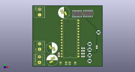
Well, core pcb corrected by all the inputs of Thor, but DEM sync layouting to be finished newt nigth, certainly external power supply for it for space area reason! Goal : everyone free to use what he has at hand already for the front end and I/V. It is 6 layers with Thorsten's layout from digital DGND to the top, so very clean about crosstalks return current paths.
layer 1 : DGND (pin14), layer 2 : +5V (pin 28: lythic decoupled to DGND layer, two C0Gs for dgnd decoupling and -15V decoupling), layer 3 : -15V (PS-pin15); layer 4 : AGND (pin5) ; layer 5 : -5V (pin26) ; layer 6 :-15V (14 DEM decoupling + decouplings of most pins towards -15V- pin 15).
It is easy to input any power supply mode : the standalone voltage source, the classic way with different secondaries
No power supply yet for the DEM sync,, I like the idea it comes from a secondary not took on the main 3 rails standalone traffo, as we do need also some +5V, +3V, etc for the digital front end !
Of course a much bigger pcb can be made, copping with all the PS and analog end and digital front end from T. ; but I think it is more prudent to begin here verroboard or wait for the GO after the proof of concept.
I am working on a less expensive to print 4 layers, certainly with 3D wires outputs like a tube amp for the current return paths not to be too much crosstalked (can be matched impedance plugs like MV Audio made on his site, etc )
On the 2 layers way, it will be hard to beat the Pedja Rogic excellent ground star layout that isolate cleverly high speed from analogs signals
But not to the decoupling of the 3 power pins in relation to each others I have found, I inputed a tweak on the AYA2/4 that is known and sounds surprisingly different . (like if the sound took testosterone but w/o loosing musicality).
I have 10 years less than you, begunn in the ennd of 90s' with that chip 🙂 ... just entghusiast way, and most with cd players, only PCB since 2014 ! (ashamed !)
Well, core pcb corrected by all the inputs of Thor, but DEM sync layouting to be finished newt nigth, certainly external power supply for it for space area reason! Goal : everyone free to use what he has at hand already for the front end and I/V. It is 6 layers with Thorsten's layout from digital DGND to the top, so very clean about crosstalks return current paths.
layer 1 : DGND (pin14), layer 2 : +5V (pin 28: lythic decoupled to DGND layer, two C0Gs for dgnd decoupling and -15V decoupling), layer 3 : -15V (PS-pin15); layer 4 : AGND (pin5) ; layer 5 : -5V (pin26) ; layer 6 :-15V (14 DEM decoupling + decouplings of most pins towards -15V- pin 15).
It is easy to input any power supply mode : the standalone voltage source, the classic way with different secondaries
No power supply yet for the DEM sync,, I like the idea it comes from a secondary not took on the main 3 rails standalone traffo, as we do need also some +5V, +3V, etc for the digital front end !
Of course a much bigger pcb can be made, copping with all the PS and analog end and digital front end from T. ; but I think it is more prudent to begin here verroboard or wait for the GO after the proof of concept.
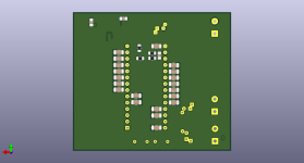
I am working on a less expensive to print 4 layers, certainly with 3D wires outputs like a tube amp for the current return paths not to be too much crosstalked (can be matched impedance plugs like MV Audio made on his site, etc )
On the 2 layers way, it will be hard to beat the Pedja Rogic excellent ground star layout that isolate cleverly high speed from analogs signals
Attachments
Last edited:
Thanks diyiggy for your response. Sorry I missed it earlier.
Well . . . I am not not sure if I agree? I did a lot of work on TDA15xx dacs in the early 90's and 2000's. (many years ago)
I always found them to be surprisingly insensitivie to PSU implementation.
Might be due to non-saturating differential CML that inherently generate low RF radiation: a light (AC) load to the PSU.
When I started - being naiv as I was then - I used the most elaborate implements I could find: multi stage Jung's Super Regulators e.t.c.
After many years of building and testing, I settled for a triplet of simple LM317's (+5, -5, -15) and passive filtering prior & post regulator - with excelllent & sonically consistent results.Well my own experience is what we use on the passive filtering affects sound greatly & I prefer using as little a value as possible for post filtering, infact if the regs are stable & low noise enough no post filtering at all.
I have some Q abut the DEM fo
1) In PHI doc staed as 176.4KHz as 4 x 44.1KHz. Did PHI refed this to use with (4 X Fs) SAA7xxx digital Oversampling filter?
Yes. Philips by default expected a free running oscillator.
Philips did not promote 4 X Fs, the comes from Henk Ten Pietrik and is based on an analysis of the DEM System, which has essentially 4 states.
By having all states within one sample, we make sure that even within one sample all errors are averaged out.
So to take advantage of this "feature" we sync the DEM clock to an external clock that is fairly low jitter and make this frequency an integer multiple of 4 X FS, so 8 X FS or 16 X FS etc. are all valid, up to a limit of around 6MHz.
I noted that in that case in principle DEM filter capacitors are not needed, all needed averaging can be left to the Analogue stage lowpass. It works (I remember John Brown tried), but I do not see it adapted that frequently. So I expect there are side effects.
Or it is Fdem independantly of F(sampling-rate) choosen? So it has to be fixed for dofferent SRs?
It can be completely independent. It can even be very low, as long as you can fit very large value (100's of uF) DEM filter capacitors that have reliably low leakage. Note that using very large electrochemical condensors for DEM filtering has poor RF behaviour.
The DEM system has 4 glitches per DEM clock cycle that have around 10-20nS width (firmly VHF) and I suspect the bit-switches have similar "dead-time". If these glitches are not dealt with right within the TDA1541 confines (filter capacitors with good RF behaviour under the IC, preferred to -15V) they will do their mischief elsewhere.
I suggested that Fdem must be either < 40Hz or > 80kHz to keep the DEM frequency breakthrough into the audio output outside the 20Hz-20khz bandwidth. I suggested also a relaxation to < 60Hz or > 60kHz would probably ok (reliably Spuria free bandwidth 30Hz-15kHz).
The 4 x is not an absolute requirement, more a functional suggestion, because of the way the DEM system works.
Or - it has to be 4 x higher from any sample rate in use?
This is my recommendation, on the principle that it is desirable to always use the lowest possible frequency for anything that is RF.
2) Does the external DEM F signal has to be present all the time, even in that time sequences when no data and Bit clock present at all?
Yes.
3) Stopped BCK opperation
Is irrelevant and counterproductive in an optimised system.
4) IF the internal DEM is present, and must be present, all of the time regardless of DATA and BCK presence, then we can sync the DEM to MCK?
Why not sync to the IIS BCK which is present before the IIS2SIM converter?
You can use MCK of course, but then your DEM Clock becomes 4 X the highest sample rate. This creates an overhead of (very) high frequency (VHF) disturbances in the system not needed for lower sample rates.
There is evidence that 64 X DEM clocks work ok, I might suggest in this case trying 64 X as DEM clock and minimal (1nF?) or no DEM filter capacitors.
From this PHI text about the DEM, it is not clear about DEM:
This mainly assumed the original, free running oscillator. This oscillator is not very stable, something presumably worse with higher frequencies and thus causing increased (T)HD at low frequencies. With sync to a stable clock this issue should disappear.
Classic DEM (470pF cap) vs Grunding DEM vs 50Hz DEM
I think non of the above are optimum.
The "low speed" DEM relies on electrochemical condensors with unreliable and unpredictable leakage specification and may require bit by bit trim for lowest HD which may be subject to seasonal average temperature changes and aging.
Grundig sync throws a lot of unnecessary noise into the DEM circuit and the -15V line. A modified version may be usable for modifying existing equipment using SAA7220.
No DEM sync causes unpredictable behaviour, which may or may be averaged out.
all refering at SIM mode setting
Stopped clock is relevant only if the clock is not correctly attenuated and slew rate limited. In this case it moves disturbances to a higher clock frequency and leaves periods without interference. But the cost is increased VHF disturbance on chip.
I think it it is best to correctly condition the input signals and to use a continuous 16X WCK bit clock.
But not to the decoupling of the 3 power pins in relation to each others
The correct way of viewing this is as contaminating the analogue reference voltage (Pin Label AGND) with noise currents from the supply lines (and DEM filtering). It is an extension of the "AGND layout is very difficult to get right" observation.
It is easy to input any power supply mode : the standalone voltage source, the classic way with different secondaries
Is not useful IMNSHO. It is counter productive. Use a single 20V supply, shunt regulated. Best on board. I recommend this:
It is an amalgam of things that were done for late prototypes of an AMR CD-77 MK II and later work on TDA1541 DAC's based on the PCB's of Thomas's Kit's.
No power supply yet for the DEM sync,
DEM Sync PSU depends on DEM sync IC's used. Signal conditioning, DEM reclock and IIS2SIM circuitry should ideally share one PSU (multiple regulators for different voltages required) and one solid ground plane linked to TDA1541 DGND with really low impedance (e.g. multiple RG-316 coax shields). All current from signal conditioning flows back to this supply anyway, so signal conditioning belongs away from TDA1541 and near the source, as does DEM reclock.
The signals for TDA1541 can run on Coax and are slew rate limited as well as limited level, so we can ignore the impedance mismatch for normal length, any connection length of < 64cm is not subject to transmission line behaviour for signals limited to 32nS slew rate.
On the 2 layers way, it will be hard to beat the Pedja Rogic excellent ground star layout that isolate cleverly high speed from analogs signals
Early versions of the CD-77 used 2 layers and star ground. Later went 4-Layer and planes, MUCH BETTER.
2 layers is simply obsolete.
Thor
- Home
- Source & Line
- Digital Line Level
- Building the ultimate NOS DAC using TDA1541A